Compare commits
31 Commits
| Author | SHA1 | Date | |
|---|---|---|---|
|
|
8bd880ce4c | ||
|
|
33d21da7f2 | ||
|
|
18901be04a | ||
|
|
9f899b96e9 | ||
|
|
88ca1910ec | ||
|
|
2f5ddbd8a3 | ||
|
|
aa5d712aea | ||
|
|
475f390a13 | ||
|
|
0731aae2bc | ||
|
|
e62abc9170 | ||
|
|
d3476139e3 | ||
|
|
8fac1cc1a0 | ||
|
|
7c91a3e0b9 | ||
|
|
fd6cff5b2b | ||
|
|
964f1903f3 | ||
|
|
12b549dafb | ||
|
|
5d5e9ff297 | ||
|
|
754d919e44 | ||
|
|
0443516cc9 | ||
|
|
5fbe0513b5 | ||
|
|
c3db8a9122 | ||
|
|
ec8256e25a | ||
|
|
8e1b3f22d2 | ||
|
|
15ae940be5 | ||
|
|
76cfc71b19 | ||
|
|
161e9a66e4 | ||
|
|
7a35f42e61 | ||
|
|
a03dd1329a | ||
|
|
6a11d33ef7 | ||
|
|
b22cadb429 | ||
|
|
f393e96d69 |
Binary file not shown.
@@ -550,7 +550,7 @@
|
|||||||
<text x="3.085225" y="81.68279375" size="1.778" layer="51">GND</text>
|
<text x="3.085225" y="81.68279375" size="1.778" layer="51">GND</text>
|
||||||
<text x="2.3" y="53.85" size="1.778" layer="51">GND</text>
|
<text x="2.3" y="53.85" size="1.778" layer="51">GND</text>
|
||||||
<text x="3.336225" y="42.247028125" size="1.778" layer="51">GND</text>
|
<text x="3.336225" y="42.247028125" size="1.778" layer="51">GND</text>
|
||||||
<text x="2.25" y="11.75" size="1.778" layer="51">GND</text>
|
<text x="2.99881875" y="12.58869375" size="1.778" layer="51">GND</text>
|
||||||
<text x="21.75" y="12.15" size="1.778" layer="51" rot="R90">GND</text>
|
<text x="21.75" y="12.15" size="1.778" layer="51" rot="R90">GND</text>
|
||||||
<text x="37.45" y="10.05" size="1.778" layer="51" rot="R90">GND</text>
|
<text x="37.45" y="10.05" size="1.778" layer="51" rot="R90">GND</text>
|
||||||
<text x="60.5" y="9.4" size="1.778" layer="51" rot="R90">GND</text>
|
<text x="60.5" y="9.4" size="1.778" layer="51" rot="R90">GND</text>
|
||||||
@@ -589,11 +589,11 @@
|
|||||||
<text x="248.95" y="49.2" size="1.778" layer="51" rot="R180">GND</text>
|
<text x="248.95" y="49.2" size="1.778" layer="51" rot="R180">GND</text>
|
||||||
<text x="248.85" y="66.55" size="1.778" layer="51" rot="R180">GND</text>
|
<text x="248.85" y="66.55" size="1.778" layer="51" rot="R180">GND</text>
|
||||||
<text x="248.8" y="82.9" size="1.778" layer="51" rot="R180">GND</text>
|
<text x="248.8" y="82.9" size="1.778" layer="51" rot="R180">GND</text>
|
||||||
<text x="256.35" y="101.95" size="1.778" layer="51" rot="R180">GND</text>
|
<text x="253.964015625" y="102.099125" size="1.778" layer="51" rot="R180">GND</text>
|
||||||
<text x="249.4" y="112.5" size="1.778" layer="51" rot="R180">GND</text>
|
<text x="249.054865625" y="112.111771875" size="1.778" layer="51" rot="R180">GND</text>
|
||||||
<text x="237.75" y="280.1" size="1.778" layer="51" rot="R270">GND</text>
|
<text x="237.75" y="280.1" size="1.778" layer="51" rot="R270">GND</text>
|
||||||
<text x="199.75" y="273.55" size="1.778" layer="51" rot="R270">GND</text>
|
<text x="199.75" y="273.55" size="1.778" layer="51" rot="R270">GND</text>
|
||||||
<text x="188.45" y="272.75" size="1.778" layer="51" rot="R270">GND</text>
|
<text x="188.539503125" y="273.018421875" size="1.778" layer="51" rot="R270">GND</text>
|
||||||
<text x="177.95" y="272.75" size="1.778" layer="51" rot="R270">GND</text>
|
<text x="177.95" y="272.75" size="1.778" layer="51" rot="R270">GND</text>
|
||||||
<text x="113.4" y="281.65" size="1.778" layer="51" rot="R270">GND</text>
|
<text x="113.4" y="281.65" size="1.778" layer="51" rot="R270">GND</text>
|
||||||
<text x="2.992190625" y="248.58331875" size="1.778" layer="51">GND</text>
|
<text x="2.992190625" y="248.58331875" size="1.778" layer="51">GND</text>
|
||||||
@@ -635,13 +635,13 @@
|
|||||||
<wire x1="161.6" y1="158.7" x2="156.95" y2="163.4" width="2.54" layer="29"/>
|
<wire x1="161.6" y1="158.7" x2="156.95" y2="163.4" width="2.54" layer="29"/>
|
||||||
<wire x1="170.1" y1="150.2" x2="165.45" y2="154.9" width="2.54" layer="29"/>
|
<wire x1="170.1" y1="150.2" x2="165.45" y2="154.9" width="2.54" layer="29"/>
|
||||||
<text x="125.137784375" y="269.740521875" size="1.778" layer="51" rot="R90">+5V0_PA_1</text>
|
<text x="125.137784375" y="269.740521875" size="1.778" layer="51" rot="R90">+5V0_PA_1</text>
|
||||||
<text x="185.45" y="267.2" size="1.778" layer="51" rot="R90">-3V4</text>
|
<text x="182.675396875" y="267.73684375" size="1.778" layer="51" rot="R90">-3V4</text>
|
||||||
<text x="196.5" y="267.4" size="1.778" layer="51" rot="R90">+3V4</text>
|
<text x="193.277878125" y="266.86315625" size="1.778" layer="51" rot="R90">+3V4</text>
|
||||||
<text x="207.4" y="267.85" size="1.778" layer="51" rot="R90">-5V0_ADAR12</text>
|
<text x="207.4" y="267.85" size="1.778" layer="51" rot="R90">-5V0_ADAR12</text>
|
||||||
<text x="188.75" y="289.05" size="1.3" layer="51" rot="R45">+3V3_ADAR12</text>
|
<text x="188.75" y="289.05" size="1.3" layer="51" rot="R45">+3V3_ADAR12</text>
|
||||||
<text x="248.25" y="270.6" size="1.778" layer="51" rot="R90">+5V0_PA_2</text>
|
<text x="248.25" y="270.6" size="1.778" layer="51" rot="R90">+5V0_PA_2</text>
|
||||||
<text x="242.8" y="98.7" size="1.778" layer="51" rot="R180">+3V4</text>
|
<text x="249.695853125" y="96.471690625" size="1.778" layer="51" rot="R180">+3V4</text>
|
||||||
<text x="242.9" y="106.65" size="1.778" layer="51" rot="R180">-3V4</text>
|
<text x="249.232640625" y="104.692303125" size="1.778" layer="51" rot="R180">-3V4</text>
|
||||||
<text x="181.4" y="99.15" size="1.778" layer="51" rot="R270">-5V0_ADAR34</text>
|
<text x="181.4" y="99.15" size="1.778" layer="51" rot="R270">-5V0_ADAR34</text>
|
||||||
<text x="185.3" y="75.15" size="1.778" layer="51" rot="R270">+3V3_ADAR34</text>
|
<text x="185.3" y="75.15" size="1.778" layer="51" rot="R270">+3V3_ADAR34</text>
|
||||||
<text x="238.95" y="72.8" size="1.778" layer="51">+3V3_VDD_SW</text>
|
<text x="238.95" y="72.8" size="1.778" layer="51">+3V3_VDD_SW</text>
|
||||||
@@ -714,8 +714,8 @@
|
|||||||
<text x="147.05" y="25.3" size="1.778" layer="51" rot="R180">CHAN14</text>
|
<text x="147.05" y="25.3" size="1.778" layer="51" rot="R180">CHAN14</text>
|
||||||
<text x="157.1" y="25.25" size="1.778" layer="51" rot="R180">CHAN15</text>
|
<text x="157.1" y="25.25" size="1.778" layer="51" rot="R180">CHAN15</text>
|
||||||
<text x="167.15" y="25.35" size="1.778" layer="51" rot="R180">CHAN16</text>
|
<text x="167.15" y="25.35" size="1.778" layer="51" rot="R180">CHAN16</text>
|
||||||
<text x="50.15" y="131.25" size="1.778" layer="51" rot="R180">SV1</text>
|
<text x="51.802165625" y="131.052934375" size="1.778" layer="51" rot="R180">SV1</text>
|
||||||
<text x="43.25" y="128.5" size="1.778" layer="51" rot="R270">VOLTAGE SEQUENCING</text>
|
<text x="35.60243125" y="132.092775" size="1.778" layer="51" rot="R270">VOLTAGE SEQUENCING</text>
|
||||||
<text x="105.55" y="106.9" size="1.2" layer="51" rot="R90">AD9523_EEPROM_SEL</text>
|
<text x="105.55" y="106.9" size="1.2" layer="51" rot="R90">AD9523_EEPROM_SEL</text>
|
||||||
<text x="107.2" y="101.85" size="1.2" layer="51" rot="R45">AD9523_STATUS0</text>
|
<text x="107.2" y="101.85" size="1.2" layer="51" rot="R45">AD9523_STATUS0</text>
|
||||||
<text x="107.25" y="99.35" size="1.2" layer="51" rot="R45">STM32_MOSI4</text>
|
<text x="107.25" y="99.35" size="1.2" layer="51" rot="R45">STM32_MOSI4</text>
|
||||||
@@ -728,20 +728,19 @@
|
|||||||
<text x="99.8" y="100.75" size="1.2" layer="51" rot="R225">STM32_MISO4</text>
|
<text x="99.8" y="100.75" size="1.2" layer="51" rot="R225">STM32_MISO4</text>
|
||||||
<text x="99.8" y="103.4" size="1.2" layer="51" rot="R225">AD9523_STATUS1</text>
|
<text x="99.8" y="103.4" size="1.2" layer="51" rot="R225">AD9523_STATUS1</text>
|
||||||
<text x="99.7" y="105.85" size="1.2" layer="51" rot="R225">GND</text>
|
<text x="99.7" y="105.85" size="1.2" layer="51" rot="R225">GND</text>
|
||||||
<text x="68.7" y="82.55" size="1.778" layer="51">JP4</text>
|
<text x="68.73355625" y="72.201796875" size="1.778" layer="51">JP4</text>
|
||||||
<text x="64.25" y="73.85" size="1.778" layer="51" rot="R270">GND</text>
|
<text x="62.77508125" y="75.956934375" size="1" layer="51" rot="R225">GND</text>
|
||||||
<text x="56.95" y="82.75" size="1.778" layer="51">JP9</text>
|
<text x="56.95" y="82.75" size="1.778" layer="51">JP9</text>
|
||||||
<text x="37.85" y="78.6" size="1.778" layer="51" rot="R90">JP2</text>
|
<text x="45.798875" y="84.61879375" size="1.778" layer="51" rot="R180">JP2</text>
|
||||||
<text x="43.95" y="88.9" size="1.778" layer="51">JP8</text>
|
<text x="43.09716875" y="85.33433125" size="1.778" layer="51" rot="R90">JP8</text>
|
||||||
<text x="29.1" y="93.2" size="1.778" layer="51">JP7</text>
|
<text x="29.1" y="93.2" size="1.778" layer="51">IMU</text>
|
||||||
<text x="21.75" y="85.35" size="1.778" layer="51">JP18</text>
|
<text x="27.568784375" y="88.61074375" size="1.778" layer="51">JP18</text>
|
||||||
<text x="89.3" y="75.5" size="1.778" layer="51" rot="R180">JP13</text>
|
<text x="89.3" y="75.5" size="1.778" layer="51" rot="R180">JP13</text>
|
||||||
<text x="75.2" y="77" size="1.778" layer="51" rot="R270">GND</text>
|
<text x="75.2" y="77" size="1.778" layer="51" rot="R270">GND</text>
|
||||||
<text x="69.6" y="74.1" size="1.778" layer="51" rot="R270">GND</text>
|
<text x="62.1909375" y="71.621040625" size="1.778" layer="51">JP10</text>
|
||||||
<text x="62.9" y="82.75" size="1.778" layer="51">JP10</text>
|
<text x="54.996875" y="70.359128125" size="1.2" layer="51">STEPPER</text>
|
||||||
<text x="53.75" y="64.4" size="1.2" layer="51" rot="R45">STEPPER_CLK+</text>
|
<text x="43.9" y="78.65" size="1.27" layer="51" rot="R270">GND</text>
|
||||||
<text x="43.9" y="78.65" size="1.778" layer="51" rot="R270">GND</text>
|
<text x="52.61158125" y="88.897171875" size="1.016" layer="51" rot="R90">GND</text>
|
||||||
<text x="53.95" y="86.4" size="1.778" layer="51">GND</text>
|
|
||||||
<text x="31.3" y="84.75" size="1.778" layer="51" rot="R270">GND</text>
|
<text x="31.3" y="84.75" size="1.778" layer="51" rot="R270">GND</text>
|
||||||
<text x="40.45" y="95.9" size="1.778" layer="51" rot="R90">GND</text>
|
<text x="40.45" y="95.9" size="1.778" layer="51" rot="R90">GND</text>
|
||||||
<rectangle x1="12.8295" y1="256.5735" x2="15.6235" y2="256.7005" layer="51"/>
|
<rectangle x1="12.8295" y1="256.5735" x2="15.6235" y2="256.7005" layer="51"/>
|
||||||
@@ -5387,6 +5386,56 @@
|
|||||||
<text x="122.221528125" y="146.5440625" size="1.27" layer="51" rot="R315">RX 3_4</text>
|
<text x="122.221528125" y="146.5440625" size="1.27" layer="51" rot="R315">RX 3_4</text>
|
||||||
<text x="145.05015" y="114.518025" size="1.27" layer="51" rot="R45">RX 4_4</text>
|
<text x="145.05015" y="114.518025" size="1.27" layer="51" rot="R45">RX 4_4</text>
|
||||||
<text x="150.25345625" y="4.79933125" size="5.4864" layer="51" font="vector">www.abac-industry.com</text>
|
<text x="150.25345625" y="4.79933125" size="5.4864" layer="51" font="vector">www.abac-industry.com</text>
|
||||||
|
<text x="47.269546875" y="127.64274375" size="1.27" layer="51" rot="R135">+1V0_FPGA</text>
|
||||||
|
<text x="47.220515625" y="125.152134375" size="1.27" layer="51" rot="R135">+1V8_FPGA</text>
|
||||||
|
<text x="47.270815625" y="122.549565625" size="1.27" layer="51" rot="R135">+3V3_FPGA</text>
|
||||||
|
<text x="47.317503125" y="119.8292125" size="1.27" layer="51" rot="R135">+5V0_ADAR</text>
|
||||||
|
<text x="47.30423125" y="117.319196875" size="1.27" layer="51" rot="R135">+3V3_ADAR12</text>
|
||||||
|
<text x="47.2552" y="114.8285875" size="1.27" layer="51" rot="R135">+3V3_ADAR34</text>
|
||||||
|
<text x="47.3055" y="112.22601875" size="1.27" layer="51" rot="R135">+3V3_ADTR</text>
|
||||||
|
<text x="47.3521875" y="109.505665625" size="1.27" layer="51" rot="R135">+3V3_SW</text>
|
||||||
|
<text x="47.262328125" y="107.0494875" size="1.27" layer="51" rot="R135">+3V3_VDD_SW</text>
|
||||||
|
<text x="47.262328125" y="104.6232625" size="1.27" layer="51" rot="R135">+5V0_PA1</text>
|
||||||
|
<text x="52.848896875" y="114.716634375" size="1.27" layer="51" rot="R315">GND</text>
|
||||||
|
<text x="52.897928125" y="117.20724375" size="1.27" layer="51" rot="R315">+3V3_CLOCK</text>
|
||||||
|
<text x="52.847628125" y="119.8098125" size="1.27" layer="51" rot="R315">+1V8_CLOCK</text>
|
||||||
|
<text x="52.800940625" y="122.530165625" size="1.27" layer="51" rot="R315">+5V5_PA</text>
|
||||||
|
<text x="52.8908" y="124.98634375" size="1.27" layer="51" rot="R315">+5V0_PA3</text>
|
||||||
|
<text x="52.8908" y="127.41256875" size="1.27" layer="51" rot="R315">+5V0_PA2</text>
|
||||||
|
<text x="52.866228125" y="112.238071875" size="1.27" layer="51" rot="R315">GND</text>
|
||||||
|
<text x="52.79689375" y="109.7075125" size="1.27" layer="51" rot="R315">GND</text>
|
||||||
|
<text x="52.7795625" y="107.038290625" size="1.27" layer="51" rot="R315">GND</text>
|
||||||
|
<text x="52.762228125" y="104.50773125" size="1.27" layer="51" rot="R315">GND</text>
|
||||||
|
<text x="37.741834375" y="95.9444" size="1.778" layer="51" rot="R90">+3V3</text>
|
||||||
|
<text x="43.11376875" y="95.9444" size="1.778" layer="51" rot="R90">SCL3</text>
|
||||||
|
<text x="45.64435" y="95.9888" size="1.778" layer="51" rot="R90">SDA3</text>
|
||||||
|
<text x="48.232090625" y="95.98181875" size="1.016" layer="51" rot="R90">MAG_DRDY</text>
|
||||||
|
<text x="50.801084375" y="95.879059375" size="1.016" layer="51" rot="R90">ACC_INT</text>
|
||||||
|
<text x="52.907659375" y="95.95613125" size="1.016" layer="51" rot="R90">GYR_INT</text>
|
||||||
|
<text x="54.502678125" y="92.739546875" size="1.778" layer="51">JP7</text>
|
||||||
|
<text x="30.45236875" y="78.6816375" size="1.778" layer="51" rot="R90">+3V3</text>
|
||||||
|
<text x="35.56853125" y="79.257065625" size="1.778" layer="51" rot="R90">SCL3</text>
|
||||||
|
<text x="38.227" y="78.789975" size="1.778" layer="51" rot="R90">SDA3</text>
|
||||||
|
<text x="39.282209375" y="78.488071875" size="1.27" layer="51" rot="R270">+3V3</text>
|
||||||
|
<text x="41.4419875" y="78.63334375" size="1.27" layer="51" rot="R270">STM32_SWCLK</text>
|
||||||
|
<text x="46.663971875" y="78.473509375" size="1.27" layer="51" rot="R270">STM32_SWDIO</text>
|
||||||
|
<text x="49.16839375" y="78.5267875" size="1.27" layer="51" rot="R270">STM32_NRST</text>
|
||||||
|
<text x="51.7793875" y="78.473509375" size="1.27" layer="51" rot="R270">STM32_SWO</text>
|
||||||
|
<text x="53.6100625" y="82.81805625" size="1.27" layer="51" rot="R315">GND</text>
|
||||||
|
<text x="53.75804375" y="77.6019375" size="1.27" layer="51" rot="R315">GND</text>
|
||||||
|
<text x="53.809425" y="80.29940625" size="1.27" layer="51" rot="R315">CW+</text>
|
||||||
|
<text x="53.520859375" y="75.467190625" size="1.27" layer="51" rot="R315">CLK+</text>
|
||||||
|
<text x="50.081" y="88.941571875" size="1.016" layer="51" rot="R90">RX5</text>
|
||||||
|
<text x="47.417228125" y="88.985971875" size="1.016" layer="51" rot="R90">TX5</text>
|
||||||
|
<text x="45.019834375" y="88.675175" size="1.016" layer="51" rot="R90">+3V3</text>
|
||||||
|
<text x="53.525646875" y="86.07393125" size="1.778" layer="51">GPS</text>
|
||||||
|
<text x="62.34479375" y="80.785540625" size="0.9" layer="51" rot="R45">EN/DIS_RFPA_VDD</text>
|
||||||
|
<text x="68.0472625" y="76.328084375" size="1" layer="51" rot="R225">GND</text>
|
||||||
|
<text x="67.5982" y="80.711553125" size="0.9" layer="51" rot="R45">EN/DIS_COOLING</text>
|
||||||
|
<text x="78.325053125" y="83.140434375" size="1.778" layer="51">ADF4382</text>
|
||||||
|
<text x="92.67903125" y="80.894575" size="1.016" layer="51">1</text>
|
||||||
|
<text x="92.77235625" y="78.2390125" size="1.016" layer="51">2</text>
|
||||||
|
<text x="73.362715625" y="77.945809375" size="1.016" layer="51">14</text>
|
||||||
</plain>
|
</plain>
|
||||||
<libraries>
|
<libraries>
|
||||||
<library name="eagle-ltspice">
|
<library name="eagle-ltspice">
|
||||||
@@ -24576,8 +24625,8 @@ Your PCBWay Team
|
|||||||
<vertex x="114" y="112" curve="-180"/>
|
<vertex x="114" y="112" curve="-180"/>
|
||||||
</polygon>
|
</polygon>
|
||||||
<polygon width="0.254" layer="1" spacing="5.08">
|
<polygon width="0.254" layer="1" spacing="5.08">
|
||||||
<vertex x="258.75" y="116" curve="-180"/>
|
<vertex x="258.9164" y="116.0208" curve="-180"/>
|
||||||
<vertex x="254.75" y="112" curve="-180"/>
|
<vertex x="254.9164" y="112.0208" curve="-180"/>
|
||||||
</polygon>
|
</polygon>
|
||||||
<polygon width="0.254" layer="1" spacing="5.08">
|
<polygon width="0.254" layer="1" spacing="5.08">
|
||||||
<vertex x="260" y="300"/>
|
<vertex x="260" y="300"/>
|
||||||
|
|||||||
File diff suppressed because it is too large
Load Diff
BIN
Binary file not shown.
Binary file not shown.
+2239
-1960
File diff suppressed because it is too large
Load Diff
+1549
-960
File diff suppressed because it is too large
Load Diff
+208673
-188312
File diff suppressed because it is too large
Load Diff
+30395
-25554
File diff suppressed because it is too large
Load Diff
+35397
-30274
File diff suppressed because it is too large
Load Diff
+208673
-188312
File diff suppressed because it is too large
Load Diff
+29185
-24314
File diff suppressed because it is too large
Load Diff
+208673
-188312
File diff suppressed because it is too large
Load Diff
+36406
-31819
File diff suppressed because it is too large
Load Diff
+172256
-151874
File diff suppressed because it is too large
Load Diff
+105
@@ -0,0 +1,105 @@
|
|||||||
|
"Qty";"Value";"Device";"Package";"Parts";"Description";"AVAILABILITY";"CHECK_PRICES";"COPYRIGHT";"DATASHEET";"DESCRIPTION";"HEIGHT";"MANUFACTURER_NAME";"MANUFACTURER_PART_NUMBER";"MF";"MFR_NAME";"MOUSER_PART_NUMBER";"MOUSER_PRICE-STOCK";"MP";"MPN";"OC_FARNELL";"OC_NEWARK";"PACKAGE";"POPULARITY";"PRICE";"PROD_ID";"REFDES";"SNAPEDA_LINK";"SPICEMODEL";"SPICEPREFIX";"TYPE";"VALUE";
|
||||||
|
"11";"";"L-EUL5650M";"L5650M";"L1, L11, L12, L13, L14, L15, L16, L17, L18, L21, L23";"INDUCTOR, European symbol";"";"";"";"";"";"";"";"";"";"";"";"";"";"";"";"";"";"0";"";"";"";"";"";"L";"";"";
|
||||||
|
"1";"";"MA10-2";"MA10-2";"SV1";"PIN HEADER";"";"";"";"";"";"";"";"";"";"";"";"";"";"";"unknown";"unknown";"";"3";"";"";"";"";"";"";"";"";
|
||||||
|
"1";"";"PINHD-1X2";"1X02";"JP20";"PIN HEADER";"";"";"";"";"";"";"";"";"";"";"";"";"";"";"";"";"";"98";"";"";"";"";"";"";"";"";
|
||||||
|
"11";"";"PINHD-1X3";"1X03";"JP4, JP5, JP6, JP10, JP11, JP12, JP14, JP15, JP16, JP17, JP19";"PIN HEADER";"";"";"";"";"";"";"";"";"";"";"";"";"";"";"";"";"";"92";"";"";"";"";"";"";"";"";
|
||||||
|
"3";"";"PINHD-1X4";"1X04";"JP8, JP9, JP18";"PIN HEADER";"";"";"";"";"";"";"";"";"";"";"";"";"";"";"";"";"";"91";"";"";"";"";"";"";"";"";
|
||||||
|
"1";"";"PINHD-1X6";"1X06";"JP2";"PIN HEADER";"";"";"";"";"";"";"";"";"";"";"";"";"";"";"";"";"";"79";"";"";"";"";"";"";"";"";
|
||||||
|
"1";"";"PINHD-1X8";"1X08";"JP7";"PIN HEADER";"";"";"";"";"";"";"";"";"";"";"";"";"";"";"";"";"";"67";"";"";"";"";"";"";"";"";
|
||||||
|
"1";"";"PINHD-2X4";"2X04";"JP3";"PIN HEADER";"";"";"";"";"";"";"";"";"";"";"";"";"";"";"";"";"";"47";"";"";"";"";"";"";"";"";
|
||||||
|
"1";"";"PINHD-2X6";"2X06";"JP1";"PIN HEADER";"";"";"";"";"";"";"";"";"";"";"";"";"";"";"";"";"";"8";"";"";"";"";"";"";"";"";
|
||||||
|
"1";"";"PINHD-2X7";"2X07";"JP13";"PIN HEADER";"";"";"";"";"";"";"";"";"";"";"";"";"";"";"";"";"";"8";"";"";"";"";"";"";"";"";
|
||||||
|
"1";"";"SJ2W";"SJ_2";"SJ1";"SMD solder JUMPER";"";"";"";"";"";"";"";"";"";"";"";"";"";"";"";"";"";"7";"";"";"";"";"";"";"";"";
|
||||||
|
"71";"0.1uF";"CC0201";"C0201";"C1, C2, C4, C5, C6, C7, C8, C9, C10, C11, C12, C13, C14, C15, C16, C36, C38, C39, C41, C42, C44, C45, C46, C47, C51, C52, C53, C56, C67, C69, C74, C80, C82, C125, C131, C133, C138, C140, C146, C148, C159, C160, C162, C168, C170, C175, C188, C189, C190, C192, C193, C194, C195, C196, C201, C203, C208, C210, C215, C217, C222, C224, C229, C231, C236, C238, C243, C245, C250, C252, C293";"CAPACITOR, European symbol";"";"";"";"";"";"";"";"";"";"";"";"";"";"";"";"";"";"";"";"";"";"";"NONE";"C";"";"";
|
||||||
|
"4";"0.1µF";"C-EUC0402";"C0402";"C48, C49, C57, C58";"CAPACITOR, European symbol";"";"";"";"";"";"";"";"";"";"";"";"";"";"";"";"";"";"18";"";"";"";"";"";"C";"";"";
|
||||||
|
"6";"0.1µF";"CC0201";"C0201";"C277, C278, C295, C297, C299, C301";"CAPACITOR, European symbol";"";"";"";"";"";"";"";"";"";"";"";"";"";"";"";"";"";"";"";"";"";"";"NONE";"C";"";"";
|
||||||
|
"1";"0.2pF";"C-EUC0201";"C0201";"C43";"CAPACITOR, European symbol";"";"";"";"";"";"";"";"";"";"";"";"";"";"";"";"";"";"0";"";"";"";"";"";"C";"";"";
|
||||||
|
"13";"0.47uF";"CC0201";"C0201";"C110, C111, C112, C113, C155, C156, C157, C158, C179, C180, C181, C182, C291";"CAPACITOR, European symbol";"";"";"";"";"";"";"";"";"";"";"";"";"";"";"";"";"";"";"";"";"";"";"NONE";"C";"";"";
|
||||||
|
"1";"0.6pF";"C-EUC0201";"C0201";"C54";"CAPACITOR, European symbol";"";"";"";"";"";"";"";"";"";"";"";"";"";"";"";"";"";"0";"";"";"";"";"";"C";"";"";
|
||||||
|
"4";"0R";"RR0201";"R0201";"R18, R19, R34, R35";"RESISTOR, European symbol";"";"";"";"";"";"";"";"";"";"";"";"";"";"";"";"";"";"";"";"";"";"";"NONE";"R";"";"";
|
||||||
|
"12";"100R";"RR0201";"R0201";"R2, R3, R4, R5, R6, R7, R8, R9, R10, R11, R12, R173";"RESISTOR, European symbol";"";"";"";"";"";"";"";"";"";"";"";"";"";"";"";"";"";"";"";"";"";"";"NONE";"R";"";"";
|
||||||
|
"28";"100nF";"C-EUC0402";"C0402";"C76, C78, C258, C259, C260, C262, C264, C266, C313, C317, C320, C324, C327, C331, C334, C337, C339, C341, C342, C343, C344, C345, C346, C347, C348, C349, C350, C351";"CAPACITOR, European symbol";"";"";"";"";"";"";"";"";"";"";"";"";"";"";"";"";"";"18";"";"";"";"";"";"C";"";"";
|
||||||
|
"24";"100nF";"CC0201";"C0201";"C24, C25, C26, C27, C28, C29, C30, C32, C33, C34, C35, C50, C256, C257, C279, C281, C298, C302, C303, C304, C305, C306, C307, C310";"CAPACITOR, European symbol";"";"";"";"";"";"";"";"";"";"";"";"";"";"";"";"";"";"";"";"";"";"";"NONE";"C";"";"";
|
||||||
|
"34";"100pF";"CC0201";"C0201";"C66, C68, C73, C79, C81, C124, C130, C132, C137, C139, C145, C147, C152, C161, C167, C169, C174, C183, C200, C202, C207, C209, C214, C216, C221, C223, C228, C230, C235, C237, C242, C244, C249, C251";"CAPACITOR, European symbol";"";"";"";"";"";"";"";"";"";"";"";"";"";"";"";"";"";"";"";"";"";"";"NONE";"C";"";"";
|
||||||
|
"2";"103pF";"CC0201";"C0201";"C60, C63";"CAPACITOR, European symbol";"";"";"";"";"";"";"";"";"";"";"";"";"";"";"";"";"";"";"";"";"";"";"NONE";"C";"";"";
|
||||||
|
"1";"106pF";"CC0201";"C0201";"C141";"CAPACITOR, European symbol";"";"";"";"";"";"";"";"";"";"";"";"";"";"";"";"";"";"";"";"";"";"";"NONE";"C";"";"";
|
||||||
|
"4";"107.3nH";"LL0201";"L0201";"L22, L25, L26, L27";"INDUCTOR, European symbol";"";"";"";"";"";"";"";"";"";"";"";"";"";"";"";"";"";"";"";"";"";"";"NONE";"L";"";"";
|
||||||
|
"9";"10k";"RR0201";"R0201";"R39, R40, R83, R84, R111, R123, R145, R151, R153";"RESISTOR, European symbol";"";"";"";"";"";"";"";"";"";"";"";"";"";"";"";"";"";"";"";"";"";"";"NONE";"R";"";"";
|
||||||
|
"16";"10nF";"CC0201";"C0201";"C102, C103, C104, C105, C106, C107, C114, C115, C116, C117, C118, C119, C120, C121, C122, C123";"CAPACITOR, European symbol";"";"";"";"";"";"";"";"";"";"";"";"";"";"";"";"";"";"";"";"";"";"";"NONE";"C";"";"";
|
||||||
|
"2";"10uF";"CC0201";"C0201";"C37, C40";"CAPACITOR, European symbol";"";"";"";"";"";"";"";"";"";"";"";"";"";"";"";"";"";"";"";"";"";"";"NONE";"C";"";"";
|
||||||
|
"12";"10µF";"C-EUC0805";"C0805";"C75, C77, C312, C316, C319, C323, C326, C330, C333, C336, C338, C340";"CAPACITOR, European symbol";"";"";"";"";"";"";"";"";"";"";"";"";"";"";"";"";"";"88";"";"";"";"";"";"C";"";"";
|
||||||
|
"1";"115R";"R-EU_R0201";"R0201";"R14";"RESISTOR, European symbol";"";"";"";"";"";"";"";"";"";"";"";"";"";"";"";"";"";"0";"";"";"";"";"";"R";"";"";
|
||||||
|
"2";"12nH";"LL0201";"L0201";"L2, L8";"INDUCTOR, European symbol";"";"";"";"";"";"";"";"";"";"";"";"";"";"";"";"";"";"";"";"";"";"";"NONE";"L";"";"";
|
||||||
|
"2";"12pF";"CC0201";"C0201";"C184, C185";"CAPACITOR, European symbol";"";"";"";"";"";"";"";"";"";"";"";"";"";"";"";"";"";"";"";"";"";"";"NONE";"C";"";"";
|
||||||
|
"37";"142-0731-211";"142-0731-211";"1420731211";"J1, J18, J20, J22, J23, J24, J25, J26, J27, J28, J29, J30, J31, J32, J33, J34, J35, J36, J37, J38, J39, J40, J41, J42, J43, J44, J45, J46, J47, J48, J49, J50, J51, J52, J53, J54, J55";"SMA Connector Jack, Female Socket 50 Ohms Through Hole Solder";"";"";"";"";"SMA Connector Jack, Female Socket 50 Ohms Through Hole Solder";"9.8852mm";"Cinch Connectivity Solutions";"142-0731-211";"";"";"530-142-0731-211";"https://www.mouser.co.uk/ProductDetail/Johnson-Cinch-Connectivity-Solutions/142-0731-211?qs=HFfMDpzxxd0OVzI3hm9tuA%3D%3D";"";"";"";"";"";"";"";"";"";"";"";"";"";"";
|
||||||
|
"2";"159nH";"LL0201";"L0201";"L3, L4";"INDUCTOR, European symbol";"";"";"";"";"";"";"";"";"";"";"";"";"";"";"";"";"";"";"";"";"";"";"NONE";"L";"";"";
|
||||||
|
"2";"18pF";"CC0201";"C0201";"C272, C274";"CAPACITOR, European symbol";"";"";"";"";"";"";"";"";"";"";"";"";"";"";"";"";"";"";"";"";"";"";"NONE";"C";"";"";
|
||||||
|
"1";"1k";"R-EU_R0402";"R0402";"R37";"RESISTOR, European symbol";"";"";"";"";"";"";"";"";"";"";"";"";"";"";"";"";"";"0";"";"";"";"";"";"R";"";"";
|
||||||
|
"49";"1k";"RR0201";"R0201";"R41, R43, R55, R56, R57, R58, R59, R61, R82, R85, R86, R87, R88, R93, R94, R99, R100, R101, R102, R107, R108, R109, R118, R124, R125, R126, R127, R128, R129, R130, R131, R133, R134, R135, R136, R137, R138, R139, R140, R144, R147, R148, R149, R167, R168, R169, R170, R171, R172";"RESISTOR, European symbol";"";"";"";"";"";"";"";"";"";"";"";"";"";"";"";"";"";"";"";"";"";"";"NONE";"R";"";"";
|
||||||
|
"1";"1k2_1%";"RR0201";"R0201";"R60";"RESISTOR, European symbol";"";"";"";"";"";"";"";"";"";"";"";"";"";"";"";"";"";"";"";"";"";"";"NONE";"R";"";"";
|
||||||
|
"7";"1nF";"C-EUC0402";"C0402";"C314, C318, C321, C325, C328, C332, C335";"CAPACITOR, European symbol";"";"";"";"";"";"";"";"";"";"";"";"";"";"";"";"";"";"18";"";"";"";"";"";"C";"";"";
|
||||||
|
"51";"1pF";"CC0201";"C0201";"C70, C71, C72, C83, C84, C85, C126, C128, C129, C134, C135, C136, C142, C143, C144, C149, C150, C151, C163, C165, C166, C171, C172, C173, C197, C198, C199, C204, C205, C206, C211, C212, C213, C218, C219, C220, C225, C226, C227, C232, C233, C234, C239, C240, C241, C246, C247, C248, C253, C254, C255";"CAPACITOR, European symbol";"";"";"";"";"";"";"";"";"";"";"";"";"";"";"";"";"";"";"";"";"";"";"NONE";"C";"";"";
|
||||||
|
"16";"1uF";"CC0201";"C0201";"C86, C87, C88, C89, C90, C91, C92, C93, C94, C95, C96, C97, C98, C99, C100, C101";"CAPACITOR, European symbol";"";"";"";"";"";"";"";"";"";"";"";"";"";"";"";"";"";"";"";"";"";"";"NONE";"C";"";"";
|
||||||
|
"3";"1µF";"CC0201";"C0201";"C276, C296, C300";"CAPACITOR, European symbol";"";"";"";"";"";"";"";"";"";"";"";"";"";"";"";"";"";"";"";"";"";"";"NONE";"C";"";"";
|
||||||
|
"1";"2.2k";"RR0201";"R0201";"R146";"RESISTOR, European symbol";"";"";"";"";"";"";"";"";"";"";"";"";"";"";"";"";"";"";"";"";"";"";"NONE";"R";"";"";
|
||||||
|
"3";"2.2uF";"CC0201";"C0201";"C22, C23, C164";"CAPACITOR, European symbol";"";"";"";"";"";"";"";"";"";"";"";"";"";"";"";"";"";"";"";"";"";"";"NONE";"C";"";"";
|
||||||
|
"16";"2.443k";"RR0201";"R0201";"R89, R90, R91, R92, R95, R96, R97, R98, R103, R104, R105, R106, R119, R120, R121, R122";"RESISTOR, European symbol";"";"";"";"";"";"";"";"";"";"";"";"";"";"";"";"";"";"";"";"";"";"";"NONE";"R";"";"";
|
||||||
|
"1";"2.7pF";"C-EUC0402";"C0402";"C3";"CAPACITOR, European symbol";"";"";"";"";"";"";"";"";"";"";"";"";"";"";"";"";"";"18";"";"";"";"";"";"C";"";"";
|
||||||
|
"2";"2.7pF";"CC0201";"C0201";"C18, C19";"CAPACITOR, European symbol";"";"";"";"";"";"";"";"";"";"";"";"";"";"";"";"";"";"";"";"";"";"";"NONE";"C";"";"";
|
||||||
|
"4";"200R";"RR0201";"R0201";"R16, R17, R20, R21";"RESISTOR, European symbol";"";"";"";"";"";"";"";"";"";"";"";"";"";"";"";"";"";"";"";"";"";"";"NONE";"R";"";"";
|
||||||
|
"1";"20k";"R-EU_R0402";"R0402";"R38";"RESISTOR, European symbol";"";"";"";"";"";"";"";"";"";"";"";"";"";"";"";"";"";"0";"";"";"";"";"";"R";"";"";
|
||||||
|
"40";"22-23-2021";"22-23-2021";"22-23-2021";"X1, X4, X5, X6, X7, X8, X9, X10, X11, X12, X13, X14, X15, X16, X17, X18, X19, X20, X21, X22, X24, X54, X55, X56, X_1, X_2, X_3, X_4, X_5, X_6, X_7, X_8, X_9, X_10, X_11, X_12, X_13, X_14, X_15, X_16";".100" (2.54mm) Center Header - 2 Pin";"";"";"";"";"";"";"";"";"MOLEX";"";"";"";"";"22-23-2021";"1462926";"25C3832";"";"40";"";"";"";"";"";"";"";"";
|
||||||
|
"16";"22-23-2031";"22-23-2031";"22-23-2031";"X3, X38, X39, X40, X41, X42, X43, X44, X45, X46, X47, X48, X49, X50, X51, X52";".100" (2.54mm) Center Header - 3 Pin";"";"";"";"";"";"";"";"";"MOLEX";"";"";"";"";"22-23-2031";"1462950";"30C0862";"";"35";"";"";"";"";"";"";"";"";
|
||||||
|
"11";"22.1k";"RR0201";"R0201";"R154, R155, R156, R157, R158, R159, R160, R161, R162, R163, R164";"RESISTOR, European symbol";"";"";"";"";"";"";"";"";"";"";"";"";"";"";"";"";"";"";"";"";"";"";"NONE";"R";"";"";
|
||||||
|
"13";"22R";"RR0201";"R0201";"R23, R24, R25, R26, R27, R28, R29, R30, R49, R51, R62, R63, R64";"RESISTOR, European symbol";"";"";"";"";"";"";"";"";"";"";"";"";"";"";"";"";"";"";"";"";"";"";"NONE";"R";"";"";
|
||||||
|
"2";"22pF";"CC0201";"C0201";"C308, C309";"CAPACITOR, European symbol";"";"";"";"";"";"";"";"";"";"";"";"";"";"";"";"";"";"";"";"";"";"";"NONE";"C";"";"";
|
||||||
|
"5";"22µF";"C-EUC1206";"C1206";"C283, C311, C315, C322, C329";"CAPACITOR, European symbol";"";"";"";"";"";"";"";"";"";"";"";"";"";"";"";"";"";"54";"";"";"";"";"";"C";"";"";
|
||||||
|
"2";"24R";"R-EU_R0402";"R0402";"R1, R13";"RESISTOR, European symbol";"";"";"";"";"";"";"";"";"";"";"";"";"";"";"";"";"";"0";"";"";"";"";"";"R";"";"";
|
||||||
|
"2";"25R";"RR0201";"R0201";"R165, R166";"RESISTOR, European symbol";"";"";"";"";"";"";"";"";"";"";"";"";"";"";"";"";"";"";"";"";"";"";"NONE";"R";"";"";
|
||||||
|
"4";"25pF";"CC0201";"C0201";"C64, C65, C268, C270";"CAPACITOR, European symbol";"";"";"";"";"";"";"";"";"";"";"";"";"";"";"";"";"";"";"";"";"";"";"NONE";"C";"";"";
|
||||||
|
"1";"3.3uF";"CC0201";"C0201";"C191";"CAPACITOR, European symbol";"";"";"";"";"";"";"";"";"";"";"";"";"";"";"";"";"";"";"";"";"";"";"NONE";"C";"";"";
|
||||||
|
"2";"32.8pF";"CC0201";"C0201";"C59, C127";"CAPACITOR, European symbol";"";"";"";"";"";"";"";"";"";"";"";"";"";"";"";"";"";"";"";"";"";"";"NONE";"C";"";"";
|
||||||
|
"1";"3k2";"RR0201";"R0201";"R33";"RESISTOR, European symbol";"";"";"";"";"";"";"";"";"";"";"";"";"";"";"";"";"";"";"";"";"";"";"NONE";"R";"";"";
|
||||||
|
"2";"4.3k";"R-EU_R0201";"R0201";"R15, R32";"RESISTOR, European symbol";"";"";"";"";"";"";"";"";"";"";"";"";"";"";"";"";"";"0";"";"";"";"";"";"R";"";"";
|
||||||
|
"2";"4.3pF";"CC0201";"C0201";"C20, C21";"CAPACITOR, European symbol";"";"";"";"";"";"";"";"";"";"";"";"";"";"";"";"";"";"";"";"";"";"";"NONE";"C";"";"";
|
||||||
|
"27";"4.7k";"RR0201";"R0201";"R42, R44, R45, R46, R47, R48, R50, R52, R53, R54, R65, R66, R67, R68, R69, R70, R71, R72, R73, R74, R75, R76, R77, R117, R141, R142, R143";"RESISTOR, European symbol";"";"";"";"";"";"";"";"";"";"";"";"";"";"";"";"";"";"";"";"";"";"";"NONE";"R";"";"";
|
||||||
|
"16";"4.7nF";"CC0201";"C0201";"C261, C263, C265, C267, C269, C271, C273, C275, C280, C282, C284, C286, C288, C290, C292, C294";"CAPACITOR, European symbol";"";"";"";"";"";"";"";"";"";"";"";"";"";"";"";"";"";"";"";"";"";"";"NONE";"C";"";"";
|
||||||
|
"8";"4.7uF";"CC0201";"C0201";"C108, C109, C153, C154, C177, C178, C287, C289";"CAPACITOR, European symbol";"";"";"";"";"";"";"";"";"";"";"";"";"";"";"";"";"";"";"";"";"";"";"NONE";"C";"";"";
|
||||||
|
"2";"4.7uF 35V";"4.7UF-POLAR-EIA3528-35V-10%(TANT)";"EIA3528";"C186, C187";"";"";"";"";"";"";"";"";"";"";"";"";"";"";"";"";"";"";"";"";"CAP-13916";"";"";"";"";"";"4.7uF 35V";
|
||||||
|
"1";"47nF";"CC0201";"C0201";"C31";"CAPACITOR, European symbol";"";"";"";"";"";"";"";"";"";"";"";"";"";"";"";"";"";"";"";"";"";"";"NONE";"C";"";"";
|
||||||
|
"4";"47uF";"CC0201";"C0201";"C17, C55, C176, C285";"CAPACITOR, European symbol";"";"";"";"";"";"";"";"";"";"";"";"";"";"";"";"";"";"";"";"";"";"";"NONE";"C";"";"";
|
||||||
|
"4";"500R";"RR0201";"R0201";"R110, R112, R113, R114";"RESISTOR, European symbol";"";"";"";"";"";"";"";"";"";"";"";"";"";"";"";"";"";"";"";"";"";"";"NONE";"R";"";"";
|
||||||
|
"3";"50R";"RR0201";"R0201";"R31, R115, R116";"RESISTOR, European symbol";"";"";"";"";"";"";"";"";"";"";"";"";"";"";"";"";"";"";"";"";"";"";"NONE";"R";"";"";
|
||||||
|
"4";"50nH";"LL0201";"L0201";"L9, L10, L24, L28";"INDUCTOR, European symbol";"";"";"";"";"";"";"";"";"";"";"";"";"";"";"";"";"";"";"";"";"";"";"NONE";"L";"";"";
|
||||||
|
"1";"56R";"R-EU_R0201";"R0201";"R22";"RESISTOR, European symbol";"";"";"";"";"";"";"";"";"";"";"";"";"";"";"";"";"";"0";"";"";"";"";"";"R";"";"";
|
||||||
|
"3";"5R";"RR0201";"R0201";"R132, R150, R152";"RESISTOR, European symbol";"";"";"";"";"";"";"";"";"";"";"";"";"";"";"";"";"";"";"";"";"";"";"NONE";"R";"";"";
|
||||||
|
"2";"7.8pF";"CC0201";"C0201";"C61, C62";"CAPACITOR, European symbol";"";"";"";"";"";"";"";"";"";"";"";"";"";"";"";"";"";"";"";"";"";"";"NONE";"C";"";"";
|
||||||
|
"1";"830R";"R-EU_R0402";"R0402";"R36";"RESISTOR, European symbol";"";"";"";"";"";"";"";"";"";"";"";"";"";"";"";"";"";"0";"";"";"";"";"";"R";"";"";
|
||||||
|
"4";"840R";"RR0201";"R0201";"R78, R79, R80, R81";"RESISTOR, European symbol";"";"";"";"";"";"";"";"";"";"";"";"";"";"";"";"";"";"";"";"";"";"";"NONE";"R";"";"";
|
||||||
|
"2";"AD8352ACPZ-R7";"AD8352ACPZ-R7";"CP_16_3_ADI";"U4, U8";"";"";"";"Copyright (C) 2025 Ultra Librarian. All rights reserved.";"https://www.analog.com/media/en/technical-documentation/data-sheets/ad8352.pdf";"2 GHz Ultralow Distortion Differential RF/IF Amplifier";"";"Analog Devices Inc";"AD8352ACPZ-R7";"";"";"";"";"";"";"";"";"";"";"";"";"";"";"";"";"";"";
|
||||||
|
"1";"AD9484BCPZ-500";"AD9484BCPZ-500";"CP_56_5_ADI";"U1";"";"";"";"Copyright (C) 2025 Ultra Librarian. All rights reserved.";"https://www.analog.com/media/en/technical-documentation/data-sheets/AD9484.pdf";"8-Bit, 500 MSPS, 1.8 V Analog-to-Digital Converter";"";"Analog Devices Inc";"AD9484BCPZ-500";"";"";"";"";"";"";"";"";"";"";"";"";"";"";"";"";"";"";
|
||||||
|
"1";"AD9708AR";"AD9708AR";"RW_28_ADI";"U3";"";"";"";"Copyright (C) 2024 Ultra Librarian. All rights reserved.";"";"";"";"";"AD9708AR";"";"Analog Devices Inc";"";"";"";"";"";"";"";"";"";"";"";"";"";"";"";"";
|
||||||
|
"4";"ADAR1000ACCZN";"ADAR1000ACCZN";"CC-88-1_ADI";"ADAR1_, ADAR2_, ADAR3_, ADAR4_";"";"";"";"Copyright (C) 2024 Ultra Librarian. All rights reserved.";"";"";"";"";"ADAR1000ACCZN";"";"Analog Devices Inc";"";"";"";"";"";"";"";"";"";"";"";"";"";"";"RF";"";
|
||||||
|
"3";"ADS7830IPWR";"ADS7830IPWR";"PW16";"U10, U88, U89";"";"";"";"Copyright (C) 2025 Ultra Librarian. All rights reserved.";"https://www.ti.com/lit/gpn/ads7830";"8-Bit, 8-Channel Sampling A/D Converter with I2C Interface 16-TSSOP -40 to 85";"";"Texas Instruments";"ADS7830IPWR";"";"";"";"";"";"";"";"";"";"";"";"";"";"";"";"";"";"";
|
||||||
|
"16";"ADTR1107ACCZ";"ADTR1107ACCZ";"CC-24-8_ADI";"ADTR1107_1, ADTR1107_2, ADTR1107_3, ADTR1107_4, ADTR1107_5, ADTR1107_6, ADTR1107_7, ADTR1107_8, ADTR1107_9, ADTR1107_10, ADTR1107_11, ADTR1107_12, ADTR1107_13, ADTR1107_14, ADTR1107_15, ADTR1107_16";"";"";"";"Copyright (C) 2024 Ultra Librarian. All rights reserved.";"";"";"";"";"ADTR1107ACCZ";"";"Analog Devices Inc";"";"";"";"";"";"";"";"";"";"";"";"";"";"";"RF";"";
|
||||||
|
"1";"AT93C46A-10SQ-2.7";"AT93C46A-10SQ-2.7";"SOIC8";"IC1";"Three-wire Automotive Temperature Serial EEPROM 1K (64 x 16)";"";"";"";"";"";"";"";"";"";"";"";"";"";"AT93C46DN-SH-B";"1455086";"58M3879";"";"0";"";"";"";"";"";"";"";"";
|
||||||
|
"5";"BLM15HB121SN1";"BLM15HB121SN1";"0402";"L5, L6, L7, L19, L20";"EMIFIL (R) Chip Ferrite Bead for GHz Noise";"";"";"";"";"";"";"";"";"";"";"";"";"";"";"";"";"";"0";"";"";"";"";"";"";"";"";
|
||||||
|
"2";"BPF2";"BPF2";"BPF2";"U$2, U$3";"";"";"";"";"";"";"";"";"";"";"";"";"";"";"";"";"";"";"";"";"";"";"";"";"";"";"";
|
||||||
|
"4";"Blue";"LED-BLUE0603";"LED-0603";"D2, D3, D4, D5";"Blue SMD LED";"";"";"";"";"";"";"";"";"";"";"";"";"";"";"";"";"";"";"";"DIO-08575";"";"";"";"";"";"Blue";
|
||||||
|
"2";"CJT-T-P-HH-ST-TH1";"CJT-T-P-HH-ST-TH1";"CJTTPHHSTTH1";"J19, J21";"Conn Twinax F 0Hz to 4GHz 100Ohm Solder ST Thru-Hole Gold";"";"";"";"";"Conn Twinax F 0Hz to 4GHz 100Ohm Solder ST Thru-Hole Gold";"7.31mm";"SAMTEC";"CJT-T-P-HH-ST-TH1";"";"";"200-CJTTPHHSTTH1";"https://www.mouser.co.uk/ProductDetail/Samtec/CJT-T-P-HH-ST-TH1?qs=PB6%2FjmICvI3dfW8RDpxn0g%3D%3D";"";"";"";"";"";"";"";"";"";"";"";"";"";"";
|
||||||
|
"2";"DAC5578SRGET";"DAC5578SRGET";"RGE24_2P7X2P7";"U7, U69";"";"";"";"Copyright (C) 2025 Ultra Librarian. All rights reserved.";"https://www.ti.com/lit/gpn/dac5578";"8-bit, Octal Channel, Ultra-Low Glitch, Voltage Output, 2-Wire Interface DAC 24-VQFN -40 to 125";"";"Texas Instruments";"DAC5578SRGET";"";"";"";"";"";"";"";"";"";"";"";"";"";"";"";"";"";"";
|
||||||
|
"1";"ECS-120-10-36B2-JTN-TR";"CRYSTAL-12MHZ";"CRYSTAL-SMD-2X2.5MM";"Y1";"12.0MHz Crystal";"";"";"";"";"";"";"";"";"";"";"";"";"";"";"";"";"";"";"";"XTAL-15540";"";"";"";"";"";"";
|
||||||
|
"1";"EP4RKU+";"EP4RKU+";"DG1677-2_MNC";"U16";"";"";"";"Copyright (C) 2024 Ultra Librarian. All rights reserved.";"";"";"";"";"EP4RKU+";"";"Mini Circuits";"";"";"";"";"";"";"";"";"";"";"";"";"";"";"";"";
|
||||||
|
"1";"FT2232HQ";"FT2232HQ";"64QFN_FT2232HQ_FTD";"U6";"";"";"";"Copyright (C) 2025 Ultra Librarian. All rights reserved.";"";"";"";"";"FT2232HQ";"";"FTDI, Future Technology Devices International Ltd";"";"";"";"";"";"";"";"";"";"";"";"";"";"";"";"";
|
||||||
|
"16";"INA241A3IDGKRDGK0008A-MFG";"INA241A3IDGKRDGK0008A-MFG";"DGK0008A-MFG";"U11, U73, U74, U75, U76, U77, U78, U79, U80, U81, U82, U83, U84, U85, U86, U87";"";"";"";"Copyright (C) 2025 Ultra Librarian. All rights reserved.";"";"-5-V to 110-V bidirectional ultraprecise current sense amplifier with enhanced PWM rejection 8-VSSOP -40 to 125";"";"Texas Instruments";"INA241A3IDGKR";"";"";"";"";"";"";"";"";"";"";"";"";"RefDes";"";"";"";"TYPE";"";
|
||||||
|
"2";"LTC5552IUDBTRMPBF";"LTC5552IUDBTRMPBF";"UDB_12_ADI";"U5, U13";"";"";"";"Copyright (C) 2024 Ultra Librarian. All rights reserved.";"";"";"";"";"LTC5552IUDB#TRMPBF";"";"Analog Devices Inc";"";"";"";"";"";"";"";"";"";"";"";"";"";"";"";"";
|
||||||
|
"17";"M3SWA2-34DR+";"M3SWA2-34DR+";"16_QFN";"RF_SW_1, RF_SW_2, RF_SW_3, RF_SW_4, RF_SW_5, RF_SW_6, RF_SW_7, RF_SW_8, RF_SW_9, RF_SW_10, RF_SW_11, RF_SW_12, RF_SW_13, RF_SW_14, RF_SW_15, RF_SW_16, U$1";"";"";"";"";"";"";"";"";"";"";"";"";"";"";"";"";"";"";"";"";"";"";"";"";"";"";"";
|
||||||
|
"2";"MINI-USB-32005-201";"MINI-USB-32005-201";"32005-201";"X2, X53";"MINI USB-B Conector";"";"";"";"";"";"";"";"";"";"";"";"";"";"";"unknown";"unknown";"";"5";"";"";"";"";"";"";"";"";
|
||||||
|
"1";"MOMENTARY-SWITCH-SPST-SMD-4.6X2.8MM";"MOMENTARY-SWITCH-SPST-SMD-4.6X2.8MM";"TACTILE_SWITCH_SMD_4.6X2.8MM";"S1";"Momentary Switch (Pushbutton) - SPST";"";"";"";"";"";"";"";"";"";"";"";"";"";"";"";"";"";"";"";"SWCH-15606";"";"";"";"";"";"";
|
||||||
|
"1";"MT25QL01GBBB8E12-0AUT";"MT25QL01GBBB8E12-0AUT";"BGA24_MT25QL_MRN";"U9";"";"";"";"Copyright (C) 2024 Ultra Librarian. All rights reserved.";"";"";"";"";"MT25QL01GBBB8E12-0AUT";"";"Micron";"";"";"";"";"";"";"";"";"";"";"";"";"";"";"";"";
|
||||||
|
"1";"NX3215SA-32.768KHz";"NX3225GD-8MHZ-STD-CRA-3";"XTAL_NX3225GD-8MHZ-STD-CRA-3_N";"XTAL3";"";"";"";"Copyright (C) 2024 Ultra Librarian. All rights reserved.";"";"";"";"";"NX3225GD-8MHZ-STD-CRA-3";"";"NDK";"";"";"";"";"";"";"";"";"";"";"";"";"";"";"";"";
|
||||||
|
"1";"NX3225GD-8MHZ-STD-CRA-3";"NX3225GD-8MHZ-STD-CRA-3";"XTAL_NX3225GD-8MHZ-STD-CRA-3_N";"XTAL1";"";"";"";"Copyright (C) 2024 Ultra Librarian. All rights reserved.";"";"";"";"";"NX3225GD-8MHZ-STD-CRA-3";"";"NDK";"";"";"";"";"";"";"";"";"";"";"";"";"";"";"";"";
|
||||||
|
"4";"OPA4703EA/250";"OPA4703EA/250";"PW14";"OPA_1, OPA_2, OPA_3, OPA_4";"";"";"";"Copyright (C) 2025 Ultra Librarian. All rights reserved.";"https://www.ti.com/lit/gpn/opa4703";"Quad, 12-V, 1-MHz, low-offset operational amplifier 14-TSSOP -40 to 85";"";"Texas Instruments";"OPA4703EA/250";"";"";"";"";"";"";"";"";"";"";"";"";"";"";"";"";"";"";
|
||||||
|
"1";"STM32F746ZGT7";"STM32F746ZGT7";"LQFP-144_STM";"U2";"";"";"";"Copyright (C) 2024 Ultra Librarian. All rights reserved.";"";"";"";"";"STM32F746ZGT7";"";"STMicroelectronics";"";"";"";"";"";"";"";"";"";"";"";"";"";"";"";"";
|
||||||
|
"34";"SZMMSZ5232BT1G";"SZMMSZ5232BT1G";"SOD-123_ONS";"U14, U15, U17, U37, U38, U39, U40, U41, U43, U44, U45, U46, U47, U48, U49, U50, U51, U52, U53, U54, U55, U56, U57, U58, U59, U60, U61, U62, U63, U64, U65, U66, U67, U68";"";"";"";"Copyright (C) 2024 Ultra Librarian. All rights reserved.";"";"";"";"";"SZMMSZ5232BT1G";"";"onsemi";"";"";"";"";"";"";"";"";"";"";"";"";"";"";"";"";
|
||||||
|
"1";"XC7A50T-2FTG256I";"XC7A50T-2FTG256I";"BGA256C100P16X16_1700X1700X155";"U42";"Artix-7 Field Programmable Gate Array (FPGA) IC 170 2764800 52160 256-LBGA Check availability";"In Stock";"https://www.snapeda.com/parts/XC7A50T-2FTG256I/Xilinx/view-part/?ref=eda";"";"";" Artix-7 Field Programmable Gate Array (FPGA) IC 170 2764800 52160 256-LBGA ";"";"";"";"Xilinx Inc.";"";"";"";"XC7A50T-2FTG256I";"";"";"";"LBGA-256 Xilinx Inc.";"";"None";"";"";"https://www.snapeda.com/parts/XC7A50T-2FTG256I/Xilinx/view-part/?ref=snap";"";"";"";"";
|
||||||
|
Can't render this file because it contains an unexpected character in line 51 and column 251.
|
+867
-521
File diff suppressed because it is too large
Load Diff
+6
-6
@@ -1,8 +1,8 @@
|
|||||||
Generated by EAGLE CAM Processor 7.4.0
|
Generated by EAGLE CAM Processor 7.4.0
|
||||||
|
|
||||||
Drill Station Info File: C:/Users/dell/Desktop/CrowdSupply/RADAR_V6/4_Schematics and Boards Layout/4_6_Schematics/MainBoard_Test/RADAR_Main_Board.dri
|
Drill Station Info File: C:/Users/dell/Desktop/CrowdSupply/RADAR_V6/4_Schematics and Boards Layout/4_6_Schematics/MainBoard_Prod_V2/RADAR_Main_Board.dri
|
||||||
|
|
||||||
Date : 06/04/2026 22:10
|
Date : 19/04/2026 23:21
|
||||||
Drills : generated
|
Drills : generated
|
||||||
Device : Excellon drill station, coordinate format 2.5 inch
|
Device : Excellon drill station, coordinate format 2.5 inch
|
||||||
|
|
||||||
@@ -27,8 +27,8 @@ Drills used:
|
|||||||
|
|
||||||
Code Size used
|
Code Size used
|
||||||
|
|
||||||
T01 0.0059inch 1609
|
T01 0.0059inch 1604
|
||||||
T02 0.0079inch 1892
|
T02 0.0079inch 2243
|
||||||
T03 0.0100inch 18
|
T03 0.0100inch 18
|
||||||
T04 0.0118inch 355
|
T04 0.0118inch 355
|
||||||
T05 0.0138inch 113
|
T05 0.0138inch 113
|
||||||
@@ -43,8 +43,8 @@ Drills used:
|
|||||||
T14 0.0472inch 4
|
T14 0.0472inch 4
|
||||||
T15 0.1260inch 8
|
T15 0.1260inch 8
|
||||||
|
|
||||||
Total number of drills: 4438
|
Total number of drills: 4784
|
||||||
|
|
||||||
Plotfiles:
|
Plotfiles:
|
||||||
|
|
||||||
C:/Users/dell/Desktop/CrowdSupply/RADAR_V6/4_Schematics and Boards Layout/4_6_Schematics/MainBoard_Test/RADAR_Main_Board.drd
|
C:/Users/dell/Desktop/CrowdSupply/RADAR_V6/4_Schematics and Boards Layout/4_6_Schematics/MainBoard_Prod_V2/RADAR_Main_Board.drd
|
||||||
|
|||||||
+3
-3
@@ -1,9 +1,9 @@
|
|||||||
Generated by EAGLE CAM Processor 7.4.0
|
Generated by EAGLE CAM Processor 7.4.0
|
||||||
|
|
||||||
Photoplotter Info File: C:/Users/dell/Desktop/CrowdSupply/RADAR_V6/4_Schematics and Boards Layout/4_6_Schematics/MainBoard_Test/RADAR_Main_Board.gpi
|
Photoplotter Info File: C:/Users/dell/Desktop/CrowdSupply/RADAR_V6/4_Schematics and Boards Layout/4_6_Schematics/MainBoard_Prod_V2/RADAR_Main_Board.gpi
|
||||||
|
|
||||||
Date : 06/04/2026 22:41
|
Date : 19/04/2026 23:50
|
||||||
Plotfile : C:/Users/dell/Desktop/CrowdSupply/RADAR_V6/4_Schematics and Boards Layout/4_6_Schematics/MainBoard_Test/RADAR_Main_Board.bsk
|
Plotfile : C:/Users/dell/Desktop/CrowdSupply/RADAR_V6/4_Schematics and Boards Layout/4_6_Schematics/MainBoard_Prod_V2/RADAR_Main_Board.bsk
|
||||||
Apertures : generated:
|
Apertures : generated:
|
||||||
Device : Gerber RS-274-X photoplotter, coordinate format 2.5 inch
|
Device : Gerber RS-274-X photoplotter, coordinate format 2.5 inch
|
||||||
|
|
||||||
|
|||||||
+13265
-9902
File diff suppressed because it is too large
Load Diff
+6728
-3421
File diff suppressed because it is too large
Load Diff
Binary file not shown.
@@ -23333,60 +23333,90 @@ X0056315Y0057299D03*
|
|||||||
X0056315Y0054937D03*
|
X0056315Y0054937D03*
|
||||||
X0056315Y0052772D03*
|
X0056315Y0052772D03*
|
||||||
X0056315Y0050606D03*
|
X0056315Y0050606D03*
|
||||||
X0057102Y0045291D03*
|
X0059477Y0051237D03*
|
||||||
X0057102Y0043126D03*
|
X0059526Y0053881D03*
|
||||||
X0057102Y0040961D03*
|
X0059526Y0056672D03*
|
||||||
X0057102Y0038992D03*
|
X0059477Y0059365D03*
|
||||||
X0057102Y0037024D03*
|
X0062171Y0059316D03*
|
||||||
X0057102Y0035055D03*
|
X0062122Y0056672D03*
|
||||||
X0059071Y0035055D03*
|
X0062219Y0053881D03*
|
||||||
X0061039Y0035055D03*
|
X0062317Y0051188D03*
|
||||||
X0061039Y0037024D03*
|
X0062268Y0048495D03*
|
||||||
X0061039Y0038992D03*
|
X0065060Y0048446D03*
|
||||||
X0059071Y0038992D03*
|
X0064913Y0051188D03*
|
||||||
X0059071Y0037024D03*
|
X0064815Y0053930D03*
|
||||||
X0059071Y0040961D03*
|
X0064913Y0056623D03*
|
||||||
X0061039Y0040961D03*
|
X0064913Y0059365D03*
|
||||||
X0063008Y0040961D03*
|
X0067655Y0056721D03*
|
||||||
X0063008Y0038992D03*
|
X0067753Y0059365D03*
|
||||||
X0063008Y0037024D03*
|
X0070251Y0059267D03*
|
||||||
X0063008Y0035055D03*
|
X0070349Y0056721D03*
|
||||||
X0064976Y0035055D03*
|
X0070251Y0053979D03*
|
||||||
X0064976Y0037024D03*
|
X0067753Y0053881D03*
|
||||||
X0064976Y0038992D03*
|
X0067704Y0051090D03*
|
||||||
X0064976Y0040961D03*
|
X0067753Y0048544D03*
|
||||||
X0066945Y0040961D03*
|
X0070300Y0048593D03*
|
||||||
X0068913Y0040961D03*
|
X0070251Y0051041D03*
|
||||||
X0068913Y0038992D03*
|
X0073835Y0050606D03*
|
||||||
X0066945Y0038992D03*
|
X0073835Y0052772D03*
|
||||||
X0066945Y0037024D03*
|
X0073835Y0055134D03*
|
||||||
X0068913Y0037024D03*
|
X0073835Y0057496D03*
|
||||||
X0068913Y0035055D03*
|
X0073835Y0059858D03*
|
||||||
X0066945Y0035055D03*
|
|
||||||
X0070882Y0035055D03*
|
|
||||||
X0072850Y0035055D03*
|
|
||||||
X0072850Y0037024D03*
|
|
||||||
X0070882Y0037024D03*
|
|
||||||
X0070882Y0038992D03*
|
|
||||||
X0072850Y0038992D03*
|
|
||||||
X0072850Y0040961D03*
|
|
||||||
X0070882Y0040961D03*
|
|
||||||
X0070882Y0043126D03*
|
|
||||||
X0072850Y0043126D03*
|
|
||||||
X0072850Y0045291D03*
|
X0072850Y0045291D03*
|
||||||
X0070882Y0045291D03*
|
X0070882Y0045291D03*
|
||||||
X0068913Y0045291D03*
|
X0070882Y0043126D03*
|
||||||
X0066945Y0045291D03*
|
X0072850Y0043126D03*
|
||||||
X0064976Y0045291D03*
|
X0072850Y0040961D03*
|
||||||
X0064976Y0043126D03*
|
X0070882Y0040961D03*
|
||||||
X0066945Y0043126D03*
|
X0070882Y0038992D03*
|
||||||
X0068913Y0043126D03*
|
X0070882Y0037024D03*
|
||||||
X0063008Y0043126D03*
|
X0072850Y0037024D03*
|
||||||
X0061039Y0043126D03*
|
X0072850Y0038992D03*
|
||||||
X0059071Y0043126D03*
|
X0072850Y0035055D03*
|
||||||
|
X0070882Y0035055D03*
|
||||||
|
X0068913Y0035055D03*
|
||||||
|
X0066945Y0035055D03*
|
||||||
|
X0066945Y0037024D03*
|
||||||
|
X0066945Y0038992D03*
|
||||||
|
X0068913Y0038992D03*
|
||||||
|
X0068913Y0037024D03*
|
||||||
|
X0068913Y0040961D03*
|
||||||
|
X0066945Y0040961D03*
|
||||||
|
X0064976Y0040961D03*
|
||||||
|
X0064976Y0038992D03*
|
||||||
|
X0064976Y0037024D03*
|
||||||
|
X0064976Y0035055D03*
|
||||||
|
X0063008Y0035055D03*
|
||||||
|
X0063008Y0037024D03*
|
||||||
|
X0063008Y0038992D03*
|
||||||
|
X0063008Y0040961D03*
|
||||||
|
X0061039Y0040961D03*
|
||||||
|
X0059071Y0040961D03*
|
||||||
|
X0059071Y0038992D03*
|
||||||
|
X0061039Y0038992D03*
|
||||||
|
X0061039Y0037024D03*
|
||||||
|
X0059071Y0037024D03*
|
||||||
|
X0059071Y0035055D03*
|
||||||
|
X0061039Y0035055D03*
|
||||||
|
X0057102Y0035055D03*
|
||||||
|
X0057102Y0037024D03*
|
||||||
|
X0057102Y0038992D03*
|
||||||
|
X0057102Y0040961D03*
|
||||||
|
X0057102Y0043126D03*
|
||||||
|
X0057102Y0045291D03*
|
||||||
X0059071Y0045291D03*
|
X0059071Y0045291D03*
|
||||||
X0061039Y0045291D03*
|
X0061039Y0045291D03*
|
||||||
X0063008Y0045291D03*
|
X0063008Y0045291D03*
|
||||||
|
X0063008Y0043126D03*
|
||||||
|
X0061039Y0043126D03*
|
||||||
|
X0059071Y0043126D03*
|
||||||
|
X0059428Y0048446D03*
|
||||||
|
X0064976Y0045291D03*
|
||||||
|
X0066945Y0045291D03*
|
||||||
|
X0068913Y0045291D03*
|
||||||
|
X0068913Y0043126D03*
|
||||||
|
X0066945Y0043126D03*
|
||||||
|
X0064976Y0043126D03*
|
||||||
X0054150Y0061630D03*
|
X0054150Y0061630D03*
|
||||||
X0051787Y0061630D03*
|
X0051787Y0061630D03*
|
||||||
X0048441Y0061630D03*
|
X0048441Y0061630D03*
|
||||||
@@ -23405,11 +23435,6 @@ X0030724Y0041157D03*
|
|||||||
X0033283Y0041157D03*
|
X0033283Y0041157D03*
|
||||||
X0035646Y0041157D03*
|
X0035646Y0041157D03*
|
||||||
X0038205Y0041157D03*
|
X0038205Y0041157D03*
|
||||||
X0073835Y0050606D03*
|
|
||||||
X0073835Y0052772D03*
|
|
||||||
X0073835Y0055134D03*
|
|
||||||
X0073835Y0057496D03*
|
|
||||||
X0073835Y0059858D03*
|
|
||||||
X0074228Y0088402D03*
|
X0074228Y0088402D03*
|
||||||
D32*
|
D32*
|
||||||
X0076000Y0051197D03*
|
X0076000Y0051197D03*
|
||||||
|
|||||||
@@ -3939,75 +3939,111 @@ X0073835Y0052772D03*
|
|||||||
X0073835Y0055134D03*
|
X0073835Y0055134D03*
|
||||||
X0073835Y0057496D03*
|
X0073835Y0057496D03*
|
||||||
X0073835Y0059858D03*
|
X0073835Y0059858D03*
|
||||||
X0066748Y0065764D03*
|
X0070251Y0059267D03*
|
||||||
X0066748Y0068126D03*
|
X0067753Y0059365D03*
|
||||||
X0066748Y0070685D03*
|
X0067655Y0056721D03*
|
||||||
X0066748Y0073244D03*
|
X0064913Y0056623D03*
|
||||||
X0066748Y0076197D03*
|
X0064815Y0053930D03*
|
||||||
X0063992Y0076197D03*
|
X0064913Y0051188D03*
|
||||||
X0063992Y0073244D03*
|
X0065060Y0048446D03*
|
||||||
X0063992Y0070685D03*
|
X0067753Y0048544D03*
|
||||||
X0063992Y0068126D03*
|
X0067704Y0051090D03*
|
||||||
|
X0070251Y0051041D03*
|
||||||
|
X0070300Y0048593D03*
|
||||||
|
X0070882Y0045291D03*
|
||||||
|
X0072850Y0045291D03*
|
||||||
|
X0072850Y0043126D03*
|
||||||
|
X0070882Y0043126D03*
|
||||||
|
X0070882Y0040961D03*
|
||||||
|
X0072850Y0040961D03*
|
||||||
|
X0072850Y0038992D03*
|
||||||
|
X0070882Y0038992D03*
|
||||||
|
X0070882Y0037024D03*
|
||||||
|
X0072850Y0037024D03*
|
||||||
|
X0072850Y0035055D03*
|
||||||
|
X0070882Y0035055D03*
|
||||||
|
X0068913Y0035055D03*
|
||||||
|
X0066945Y0035055D03*
|
||||||
|
X0066945Y0037024D03*
|
||||||
|
X0066945Y0038992D03*
|
||||||
|
X0068913Y0038992D03*
|
||||||
|
X0068913Y0037024D03*
|
||||||
|
X0068913Y0040961D03*
|
||||||
|
X0066945Y0040961D03*
|
||||||
|
X0064976Y0040961D03*
|
||||||
|
X0064976Y0038992D03*
|
||||||
|
X0064976Y0037024D03*
|
||||||
|
X0064976Y0035055D03*
|
||||||
|
X0063008Y0035055D03*
|
||||||
|
X0063008Y0037024D03*
|
||||||
|
X0063008Y0038992D03*
|
||||||
|
X0063008Y0040961D03*
|
||||||
|
X0061039Y0040961D03*
|
||||||
|
X0059071Y0040961D03*
|
||||||
|
X0059071Y0038992D03*
|
||||||
|
X0061039Y0038992D03*
|
||||||
|
X0061039Y0037024D03*
|
||||||
|
X0059071Y0037024D03*
|
||||||
|
X0059071Y0035055D03*
|
||||||
|
X0061039Y0035055D03*
|
||||||
|
X0057102Y0035055D03*
|
||||||
|
X0057102Y0037024D03*
|
||||||
|
X0057102Y0038992D03*
|
||||||
|
X0057102Y0040961D03*
|
||||||
|
X0057102Y0043126D03*
|
||||||
|
X0057102Y0045291D03*
|
||||||
|
X0059071Y0045291D03*
|
||||||
|
X0061039Y0045291D03*
|
||||||
|
X0063008Y0045291D03*
|
||||||
|
X0063008Y0043126D03*
|
||||||
|
X0061039Y0043126D03*
|
||||||
|
X0059071Y0043126D03*
|
||||||
|
X0059428Y0048446D03*
|
||||||
|
X0059477Y0051237D03*
|
||||||
|
X0059526Y0053881D03*
|
||||||
|
X0059526Y0056672D03*
|
||||||
|
X0059477Y0059365D03*
|
||||||
|
X0062171Y0059316D03*
|
||||||
|
X0062122Y0056672D03*
|
||||||
|
X0062219Y0053881D03*
|
||||||
|
X0062317Y0051188D03*
|
||||||
|
X0062268Y0048495D03*
|
||||||
|
X0064976Y0045291D03*
|
||||||
|
X0066945Y0045291D03*
|
||||||
|
X0068913Y0045291D03*
|
||||||
|
X0068913Y0043126D03*
|
||||||
|
X0066945Y0043126D03*
|
||||||
|
X0064976Y0043126D03*
|
||||||
|
X0067753Y0053881D03*
|
||||||
|
X0070251Y0053979D03*
|
||||||
|
X0070349Y0056721D03*
|
||||||
|
X0064913Y0059365D03*
|
||||||
X0063992Y0065764D03*
|
X0063992Y0065764D03*
|
||||||
|
X0063992Y0068126D03*
|
||||||
|
X0063992Y0070685D03*
|
||||||
|
X0063992Y0073244D03*
|
||||||
|
X0063992Y0076197D03*
|
||||||
|
X0066748Y0076197D03*
|
||||||
|
X0066748Y0073244D03*
|
||||||
|
X0066748Y0070685D03*
|
||||||
|
X0066748Y0068126D03*
|
||||||
|
X0066748Y0065764D03*
|
||||||
|
X0066551Y0079937D03*
|
||||||
|
X0066551Y0083087D03*
|
||||||
|
X0067535Y0085843D03*
|
||||||
|
X0064583Y0086433D03*
|
||||||
|
X0063795Y0083283D03*
|
||||||
|
X0063992Y0079937D03*
|
||||||
|
X0069307Y0082693D03*
|
||||||
|
X0071276Y0085449D03*
|
||||||
|
X0070094Y0088598D03*
|
||||||
|
X0066748Y0088992D03*
|
||||||
|
X0074228Y0088402D03*
|
||||||
X0056315Y0059661D03*
|
X0056315Y0059661D03*
|
||||||
X0056315Y0057299D03*
|
X0056315Y0057299D03*
|
||||||
X0056315Y0054937D03*
|
X0056315Y0054937D03*
|
||||||
X0056315Y0052772D03*
|
X0056315Y0052772D03*
|
||||||
X0056315Y0050606D03*
|
X0056315Y0050606D03*
|
||||||
X0057102Y0045291D03*
|
|
||||||
X0057102Y0043126D03*
|
|
||||||
X0057102Y0040961D03*
|
|
||||||
X0057102Y0038992D03*
|
|
||||||
X0057102Y0037024D03*
|
|
||||||
X0057102Y0035055D03*
|
|
||||||
X0059071Y0035055D03*
|
|
||||||
X0061039Y0035055D03*
|
|
||||||
X0061039Y0037024D03*
|
|
||||||
X0061039Y0038992D03*
|
|
||||||
X0059071Y0038992D03*
|
|
||||||
X0059071Y0037024D03*
|
|
||||||
X0059071Y0040961D03*
|
|
||||||
X0061039Y0040961D03*
|
|
||||||
X0063008Y0040961D03*
|
|
||||||
X0063008Y0038992D03*
|
|
||||||
X0063008Y0037024D03*
|
|
||||||
X0063008Y0035055D03*
|
|
||||||
X0064976Y0035055D03*
|
|
||||||
X0064976Y0037024D03*
|
|
||||||
X0064976Y0038992D03*
|
|
||||||
X0064976Y0040961D03*
|
|
||||||
X0066945Y0040961D03*
|
|
||||||
X0068913Y0040961D03*
|
|
||||||
X0068913Y0038992D03*
|
|
||||||
X0066945Y0038992D03*
|
|
||||||
X0066945Y0037024D03*
|
|
||||||
X0068913Y0037024D03*
|
|
||||||
X0068913Y0035055D03*
|
|
||||||
X0066945Y0035055D03*
|
|
||||||
X0070882Y0035055D03*
|
|
||||||
X0072850Y0035055D03*
|
|
||||||
X0072850Y0037024D03*
|
|
||||||
X0070882Y0037024D03*
|
|
||||||
X0070882Y0038992D03*
|
|
||||||
X0072850Y0038992D03*
|
|
||||||
X0072850Y0040961D03*
|
|
||||||
X0070882Y0040961D03*
|
|
||||||
X0070882Y0043126D03*
|
|
||||||
X0072850Y0043126D03*
|
|
||||||
X0072850Y0045291D03*
|
|
||||||
X0070882Y0045291D03*
|
|
||||||
X0068913Y0045291D03*
|
|
||||||
X0066945Y0045291D03*
|
|
||||||
X0064976Y0045291D03*
|
|
||||||
X0064976Y0043126D03*
|
|
||||||
X0066945Y0043126D03*
|
|
||||||
X0068913Y0043126D03*
|
|
||||||
X0063008Y0043126D03*
|
|
||||||
X0061039Y0043126D03*
|
|
||||||
X0059071Y0043126D03*
|
|
||||||
X0059071Y0045291D03*
|
|
||||||
X0061039Y0045291D03*
|
|
||||||
X0063008Y0045291D03*
|
|
||||||
X0054150Y0061630D03*
|
X0054150Y0061630D03*
|
||||||
X0051787Y0061630D03*
|
X0051787Y0061630D03*
|
||||||
X0048441Y0061630D03*
|
X0048441Y0061630D03*
|
||||||
@@ -4026,40 +4062,29 @@ X0030724Y0041157D03*
|
|||||||
X0033283Y0041157D03*
|
X0033283Y0041157D03*
|
||||||
X0035646Y0041157D03*
|
X0035646Y0041157D03*
|
||||||
X0038205Y0041157D03*
|
X0038205Y0041157D03*
|
||||||
X0063992Y0079937D03*
|
|
||||||
X0063795Y0083283D03*
|
|
||||||
X0066551Y0083087D03*
|
|
||||||
X0067535Y0085843D03*
|
|
||||||
X0064583Y0086433D03*
|
|
||||||
X0066748Y0088992D03*
|
|
||||||
X0070094Y0088598D03*
|
|
||||||
X0071276Y0085449D03*
|
|
||||||
X0069307Y0082693D03*
|
|
||||||
X0066551Y0079937D03*
|
|
||||||
X0074228Y0088402D03*
|
|
||||||
D16*
|
D16*
|
||||||
X0076000Y0051197D03*
|
|
||||||
X0079937Y0051197D03*
|
|
||||||
X0083874Y0051197D03*
|
|
||||||
X0087811Y0051197D03*
|
|
||||||
X0091748Y0051197D03*
|
|
||||||
X0095685Y0051197D03*
|
|
||||||
X0095685Y0044685D03*
|
|
||||||
X0091748Y0045276D03*
|
|
||||||
X0087811Y0045276D03*
|
|
||||||
X0083874Y0045276D03*
|
|
||||||
X0079937Y0045276D03*
|
|
||||||
X0076000Y0045276D03*
|
|
||||||
X0054150Y0045079D03*
|
|
||||||
X0050213Y0045079D03*
|
|
||||||
X0046276Y0045079D03*
|
|
||||||
X0042339Y0045079D03*
|
|
||||||
X0038402Y0045079D03*
|
X0038402Y0045079D03*
|
||||||
X0034465Y0045079D03*
|
X0042339Y0045079D03*
|
||||||
X0034465Y0051000D03*
|
X0046276Y0045079D03*
|
||||||
X0038402Y0051000D03*
|
X0050213Y0045079D03*
|
||||||
X0042339Y0051000D03*
|
X0054150Y0045079D03*
|
||||||
X0046276Y0051000D03*
|
|
||||||
X0050213Y0051000D03*
|
|
||||||
X0054150Y0051000D03*
|
X0054150Y0051000D03*
|
||||||
|
X0050213Y0051000D03*
|
||||||
|
X0046276Y0051000D03*
|
||||||
|
X0042339Y0051000D03*
|
||||||
|
X0038402Y0051000D03*
|
||||||
|
X0034465Y0051000D03*
|
||||||
|
X0034465Y0045079D03*
|
||||||
|
X0076000Y0045276D03*
|
||||||
|
X0079937Y0045276D03*
|
||||||
|
X0083874Y0045276D03*
|
||||||
|
X0087811Y0045276D03*
|
||||||
|
X0091748Y0045276D03*
|
||||||
|
X0095685Y0044685D03*
|
||||||
|
X0095685Y0051197D03*
|
||||||
|
X0091748Y0051197D03*
|
||||||
|
X0087811Y0051197D03*
|
||||||
|
X0083874Y0051197D03*
|
||||||
|
X0079937Y0051197D03*
|
||||||
|
X0076000Y0051197D03*
|
||||||
M02*
|
M02*
|
||||||
|
|||||||
@@ -4066,75 +4066,111 @@ X0073835Y0052772D03*
|
|||||||
X0073835Y0055134D03*
|
X0073835Y0055134D03*
|
||||||
X0073835Y0057496D03*
|
X0073835Y0057496D03*
|
||||||
X0073835Y0059858D03*
|
X0073835Y0059858D03*
|
||||||
X0066748Y0065764D03*
|
X0070251Y0059267D03*
|
||||||
X0066748Y0068126D03*
|
X0067753Y0059365D03*
|
||||||
X0066748Y0070685D03*
|
X0067655Y0056721D03*
|
||||||
X0066748Y0073244D03*
|
X0064913Y0056623D03*
|
||||||
X0066748Y0076197D03*
|
X0064815Y0053930D03*
|
||||||
X0063992Y0076197D03*
|
X0064913Y0051188D03*
|
||||||
X0063992Y0073244D03*
|
X0065060Y0048446D03*
|
||||||
X0063992Y0070685D03*
|
X0067753Y0048544D03*
|
||||||
X0063992Y0068126D03*
|
X0067704Y0051090D03*
|
||||||
|
X0070251Y0051041D03*
|
||||||
|
X0070300Y0048593D03*
|
||||||
|
X0070882Y0045291D03*
|
||||||
|
X0072850Y0045291D03*
|
||||||
|
X0072850Y0043126D03*
|
||||||
|
X0070882Y0043126D03*
|
||||||
|
X0070882Y0040961D03*
|
||||||
|
X0072850Y0040961D03*
|
||||||
|
X0072850Y0038992D03*
|
||||||
|
X0070882Y0038992D03*
|
||||||
|
X0070882Y0037024D03*
|
||||||
|
X0072850Y0037024D03*
|
||||||
|
X0072850Y0035055D03*
|
||||||
|
X0070882Y0035055D03*
|
||||||
|
X0068913Y0035055D03*
|
||||||
|
X0066945Y0035055D03*
|
||||||
|
X0066945Y0037024D03*
|
||||||
|
X0066945Y0038992D03*
|
||||||
|
X0068913Y0038992D03*
|
||||||
|
X0068913Y0037024D03*
|
||||||
|
X0068913Y0040961D03*
|
||||||
|
X0066945Y0040961D03*
|
||||||
|
X0064976Y0040961D03*
|
||||||
|
X0064976Y0038992D03*
|
||||||
|
X0064976Y0037024D03*
|
||||||
|
X0064976Y0035055D03*
|
||||||
|
X0063008Y0035055D03*
|
||||||
|
X0063008Y0037024D03*
|
||||||
|
X0063008Y0038992D03*
|
||||||
|
X0063008Y0040961D03*
|
||||||
|
X0061039Y0040961D03*
|
||||||
|
X0059071Y0040961D03*
|
||||||
|
X0059071Y0038992D03*
|
||||||
|
X0061039Y0038992D03*
|
||||||
|
X0061039Y0037024D03*
|
||||||
|
X0059071Y0037024D03*
|
||||||
|
X0059071Y0035055D03*
|
||||||
|
X0061039Y0035055D03*
|
||||||
|
X0057102Y0035055D03*
|
||||||
|
X0057102Y0037024D03*
|
||||||
|
X0057102Y0038992D03*
|
||||||
|
X0057102Y0040961D03*
|
||||||
|
X0057102Y0043126D03*
|
||||||
|
X0057102Y0045291D03*
|
||||||
|
X0059071Y0045291D03*
|
||||||
|
X0061039Y0045291D03*
|
||||||
|
X0063008Y0045291D03*
|
||||||
|
X0063008Y0043126D03*
|
||||||
|
X0061039Y0043126D03*
|
||||||
|
X0059071Y0043126D03*
|
||||||
|
X0059428Y0048446D03*
|
||||||
|
X0059477Y0051237D03*
|
||||||
|
X0059526Y0053881D03*
|
||||||
|
X0059526Y0056672D03*
|
||||||
|
X0059477Y0059365D03*
|
||||||
|
X0062171Y0059316D03*
|
||||||
|
X0062122Y0056672D03*
|
||||||
|
X0062219Y0053881D03*
|
||||||
|
X0062317Y0051188D03*
|
||||||
|
X0062268Y0048495D03*
|
||||||
|
X0064976Y0045291D03*
|
||||||
|
X0066945Y0045291D03*
|
||||||
|
X0068913Y0045291D03*
|
||||||
|
X0068913Y0043126D03*
|
||||||
|
X0066945Y0043126D03*
|
||||||
|
X0064976Y0043126D03*
|
||||||
|
X0067753Y0053881D03*
|
||||||
|
X0070251Y0053979D03*
|
||||||
|
X0070349Y0056721D03*
|
||||||
|
X0064913Y0059365D03*
|
||||||
X0063992Y0065764D03*
|
X0063992Y0065764D03*
|
||||||
|
X0063992Y0068126D03*
|
||||||
|
X0063992Y0070685D03*
|
||||||
|
X0063992Y0073244D03*
|
||||||
|
X0063992Y0076197D03*
|
||||||
|
X0066748Y0076197D03*
|
||||||
|
X0066748Y0073244D03*
|
||||||
|
X0066748Y0070685D03*
|
||||||
|
X0066748Y0068126D03*
|
||||||
|
X0066748Y0065764D03*
|
||||||
|
X0066551Y0079937D03*
|
||||||
|
X0066551Y0083087D03*
|
||||||
|
X0067535Y0085843D03*
|
||||||
|
X0064583Y0086433D03*
|
||||||
|
X0063795Y0083283D03*
|
||||||
|
X0063992Y0079937D03*
|
||||||
|
X0069307Y0082693D03*
|
||||||
|
X0071276Y0085449D03*
|
||||||
|
X0070094Y0088598D03*
|
||||||
|
X0066748Y0088992D03*
|
||||||
|
X0074228Y0088402D03*
|
||||||
X0056315Y0059661D03*
|
X0056315Y0059661D03*
|
||||||
X0056315Y0057299D03*
|
X0056315Y0057299D03*
|
||||||
X0056315Y0054937D03*
|
X0056315Y0054937D03*
|
||||||
X0056315Y0052772D03*
|
X0056315Y0052772D03*
|
||||||
X0056315Y0050606D03*
|
X0056315Y0050606D03*
|
||||||
X0057102Y0045291D03*
|
|
||||||
X0057102Y0043126D03*
|
|
||||||
X0057102Y0040961D03*
|
|
||||||
X0057102Y0038992D03*
|
|
||||||
X0057102Y0037024D03*
|
|
||||||
X0057102Y0035055D03*
|
|
||||||
X0059071Y0035055D03*
|
|
||||||
X0061039Y0035055D03*
|
|
||||||
X0061039Y0037024D03*
|
|
||||||
X0061039Y0038992D03*
|
|
||||||
X0059071Y0038992D03*
|
|
||||||
X0059071Y0037024D03*
|
|
||||||
X0059071Y0040961D03*
|
|
||||||
X0061039Y0040961D03*
|
|
||||||
X0063008Y0040961D03*
|
|
||||||
X0063008Y0038992D03*
|
|
||||||
X0063008Y0037024D03*
|
|
||||||
X0063008Y0035055D03*
|
|
||||||
X0064976Y0035055D03*
|
|
||||||
X0064976Y0037024D03*
|
|
||||||
X0064976Y0038992D03*
|
|
||||||
X0064976Y0040961D03*
|
|
||||||
X0066945Y0040961D03*
|
|
||||||
X0068913Y0040961D03*
|
|
||||||
X0068913Y0038992D03*
|
|
||||||
X0066945Y0038992D03*
|
|
||||||
X0066945Y0037024D03*
|
|
||||||
X0068913Y0037024D03*
|
|
||||||
X0068913Y0035055D03*
|
|
||||||
X0066945Y0035055D03*
|
|
||||||
X0070882Y0035055D03*
|
|
||||||
X0072850Y0035055D03*
|
|
||||||
X0072850Y0037024D03*
|
|
||||||
X0070882Y0037024D03*
|
|
||||||
X0070882Y0038992D03*
|
|
||||||
X0072850Y0038992D03*
|
|
||||||
X0072850Y0040961D03*
|
|
||||||
X0070882Y0040961D03*
|
|
||||||
X0070882Y0043126D03*
|
|
||||||
X0072850Y0043126D03*
|
|
||||||
X0072850Y0045291D03*
|
|
||||||
X0070882Y0045291D03*
|
|
||||||
X0068913Y0045291D03*
|
|
||||||
X0066945Y0045291D03*
|
|
||||||
X0064976Y0045291D03*
|
|
||||||
X0064976Y0043126D03*
|
|
||||||
X0066945Y0043126D03*
|
|
||||||
X0068913Y0043126D03*
|
|
||||||
X0063008Y0043126D03*
|
|
||||||
X0061039Y0043126D03*
|
|
||||||
X0059071Y0043126D03*
|
|
||||||
X0059071Y0045291D03*
|
|
||||||
X0061039Y0045291D03*
|
|
||||||
X0063008Y0045291D03*
|
|
||||||
X0054150Y0061630D03*
|
X0054150Y0061630D03*
|
||||||
X0051787Y0061630D03*
|
X0051787Y0061630D03*
|
||||||
X0048441Y0061630D03*
|
X0048441Y0061630D03*
|
||||||
@@ -4153,40 +4189,29 @@ X0030724Y0041157D03*
|
|||||||
X0033283Y0041157D03*
|
X0033283Y0041157D03*
|
||||||
X0035646Y0041157D03*
|
X0035646Y0041157D03*
|
||||||
X0038205Y0041157D03*
|
X0038205Y0041157D03*
|
||||||
X0063992Y0079937D03*
|
|
||||||
X0063795Y0083283D03*
|
|
||||||
X0066551Y0083087D03*
|
|
||||||
X0067535Y0085843D03*
|
|
||||||
X0064583Y0086433D03*
|
|
||||||
X0066748Y0088992D03*
|
|
||||||
X0070094Y0088598D03*
|
|
||||||
X0071276Y0085449D03*
|
|
||||||
X0069307Y0082693D03*
|
|
||||||
X0066551Y0079937D03*
|
|
||||||
X0074228Y0088402D03*
|
|
||||||
D16*
|
D16*
|
||||||
X0076000Y0051197D03*
|
|
||||||
X0079937Y0051197D03*
|
|
||||||
X0083874Y0051197D03*
|
|
||||||
X0087811Y0051197D03*
|
|
||||||
X0091748Y0051197D03*
|
|
||||||
X0095685Y0051197D03*
|
|
||||||
X0095685Y0044685D03*
|
|
||||||
X0091748Y0045276D03*
|
|
||||||
X0087811Y0045276D03*
|
|
||||||
X0083874Y0045276D03*
|
|
||||||
X0079937Y0045276D03*
|
|
||||||
X0076000Y0045276D03*
|
|
||||||
X0054150Y0045079D03*
|
|
||||||
X0050213Y0045079D03*
|
|
||||||
X0046276Y0045079D03*
|
|
||||||
X0042339Y0045079D03*
|
|
||||||
X0038402Y0045079D03*
|
X0038402Y0045079D03*
|
||||||
X0034465Y0045079D03*
|
X0042339Y0045079D03*
|
||||||
X0034465Y0051000D03*
|
X0046276Y0045079D03*
|
||||||
X0038402Y0051000D03*
|
X0050213Y0045079D03*
|
||||||
X0042339Y0051000D03*
|
X0054150Y0045079D03*
|
||||||
X0046276Y0051000D03*
|
|
||||||
X0050213Y0051000D03*
|
|
||||||
X0054150Y0051000D03*
|
X0054150Y0051000D03*
|
||||||
|
X0050213Y0051000D03*
|
||||||
|
X0046276Y0051000D03*
|
||||||
|
X0042339Y0051000D03*
|
||||||
|
X0038402Y0051000D03*
|
||||||
|
X0034465Y0051000D03*
|
||||||
|
X0034465Y0045079D03*
|
||||||
|
X0076000Y0045276D03*
|
||||||
|
X0079937Y0045276D03*
|
||||||
|
X0083874Y0045276D03*
|
||||||
|
X0087811Y0045276D03*
|
||||||
|
X0091748Y0045276D03*
|
||||||
|
X0095685Y0044685D03*
|
||||||
|
X0095685Y0051197D03*
|
||||||
|
X0091748Y0051197D03*
|
||||||
|
X0087811Y0051197D03*
|
||||||
|
X0083874Y0051197D03*
|
||||||
|
X0079937Y0051197D03*
|
||||||
|
X0076000Y0051197D03*
|
||||||
M02*
|
M02*
|
||||||
|
|||||||
@@ -33,60 +33,30 @@ X56315Y57299
|
|||||||
X56315Y54937
|
X56315Y54937
|
||||||
X56315Y52772
|
X56315Y52772
|
||||||
X56315Y50606
|
X56315Y50606
|
||||||
X57102Y45291
|
X59477Y51237
|
||||||
X57102Y43126
|
X59526Y53881
|
||||||
X57102Y40961
|
X59526Y56672
|
||||||
X57102Y38992
|
X59477Y59365
|
||||||
X57102Y37024
|
X62171Y59316
|
||||||
X57102Y35055
|
X62122Y56672
|
||||||
X59071Y35055
|
X62219Y53881
|
||||||
X61039Y35055
|
X62317Y51188
|
||||||
X61039Y37024
|
X62268Y48495
|
||||||
X61039Y38992
|
X65060Y48446
|
||||||
X59071Y38992
|
X64913Y51188
|
||||||
X59071Y37024
|
X64815Y53930
|
||||||
X59071Y40961
|
X64913Y56623
|
||||||
X61039Y40961
|
X64913Y59365
|
||||||
X63008Y40961
|
X67655Y56721
|
||||||
X63008Y38992
|
X67753Y59365
|
||||||
X63008Y37024
|
X70251Y59267
|
||||||
X63008Y35055
|
X70349Y56721
|
||||||
X64976Y35055
|
X70251Y53979
|
||||||
X64976Y37024
|
X67753Y53881
|
||||||
X64976Y38992
|
X67704Y51090
|
||||||
X64976Y40961
|
X67753Y48544
|
||||||
X66945Y40961
|
X70300Y48593
|
||||||
X68913Y40961
|
X70251Y51041
|
||||||
X68913Y38992
|
|
||||||
X66945Y38992
|
|
||||||
X66945Y37024
|
|
||||||
X68913Y37024
|
|
||||||
X68913Y35055
|
|
||||||
X66945Y35055
|
|
||||||
X70882Y35055
|
|
||||||
X72850Y35055
|
|
||||||
X72850Y37024
|
|
||||||
X70882Y37024
|
|
||||||
X70882Y38992
|
|
||||||
X72850Y38992
|
|
||||||
X72850Y40961
|
|
||||||
X70882Y40961
|
|
||||||
X70882Y43126
|
|
||||||
X72850Y43126
|
|
||||||
X72850Y45291
|
|
||||||
X70882Y45291
|
|
||||||
X68913Y45291
|
|
||||||
X66945Y45291
|
|
||||||
X64976Y45291
|
|
||||||
X64976Y43126
|
|
||||||
X66945Y43126
|
|
||||||
X68913Y43126
|
|
||||||
X63008Y43126
|
|
||||||
X61039Y43126
|
|
||||||
X59071Y43126
|
|
||||||
X59071Y45291
|
|
||||||
X61039Y45291
|
|
||||||
X63008Y45291
|
|
||||||
X73835Y50606
|
X73835Y50606
|
||||||
X73835Y52772
|
X73835Y52772
|
||||||
X73835Y55134
|
X73835Y55134
|
||||||
@@ -113,19 +83,62 @@ X71276Y85449
|
|||||||
X69307Y82693
|
X69307Y82693
|
||||||
X66551Y79937
|
X66551Y79937
|
||||||
X74228Y88402
|
X74228Y88402
|
||||||
|
X59428Y48446
|
||||||
|
X59071Y45291
|
||||||
|
X61039Y45291
|
||||||
|
X63008Y45291
|
||||||
|
X63008Y43126
|
||||||
|
X61039Y43126
|
||||||
|
X59071Y43126
|
||||||
|
X59071Y40961
|
||||||
|
X61039Y40961
|
||||||
|
X61039Y38992
|
||||||
|
X59071Y38992
|
||||||
|
X59071Y37024
|
||||||
|
X61039Y37024
|
||||||
|
X63008Y37024
|
||||||
|
X63008Y38992
|
||||||
|
X63008Y40961
|
||||||
|
X64976Y40961
|
||||||
|
X64976Y38992
|
||||||
|
X64976Y37024
|
||||||
|
X64976Y35055
|
||||||
|
X66945Y35055
|
||||||
|
X68913Y35055
|
||||||
|
X68913Y37024
|
||||||
|
X68913Y38992
|
||||||
|
X66945Y38992
|
||||||
|
X66945Y37024
|
||||||
|
X66945Y40961
|
||||||
|
X68913Y40961
|
||||||
|
X68913Y43126
|
||||||
|
X66945Y43126
|
||||||
|
X64976Y43126
|
||||||
|
X64976Y45291
|
||||||
|
X66945Y45291
|
||||||
|
X68913Y45291
|
||||||
|
X70882Y45291
|
||||||
|
X72850Y45291
|
||||||
|
X72850Y43126
|
||||||
|
X70882Y43126
|
||||||
|
X70882Y40961
|
||||||
|
X72850Y40961
|
||||||
|
X72850Y38992
|
||||||
|
X70882Y38992
|
||||||
|
X70882Y37024
|
||||||
|
X72850Y37024
|
||||||
|
X72850Y35055
|
||||||
|
X70882Y35055
|
||||||
|
X63008Y35055
|
||||||
|
X61039Y35055
|
||||||
|
X59071Y35055
|
||||||
|
X57102Y35055
|
||||||
|
X57102Y37024
|
||||||
|
X57102Y38992
|
||||||
|
X57102Y40961
|
||||||
|
X57102Y43126
|
||||||
|
X57102Y45291
|
||||||
T02
|
T02
|
||||||
X76000Y51197
|
|
||||||
X79937Y51197
|
|
||||||
X83874Y51197
|
|
||||||
X87811Y51197
|
|
||||||
X91748Y51197
|
|
||||||
X95685Y51197
|
|
||||||
X95685Y44685
|
|
||||||
X91748Y45276
|
|
||||||
X87811Y45276
|
|
||||||
X83874Y45276
|
|
||||||
X79937Y45276
|
|
||||||
X76000Y45276
|
|
||||||
X54150Y45079
|
X54150Y45079
|
||||||
X50213Y45079
|
X50213Y45079
|
||||||
X46276Y45079
|
X46276Y45079
|
||||||
@@ -138,24 +151,25 @@ X42339Y51000
|
|||||||
X46276Y51000
|
X46276Y51000
|
||||||
X50213Y51000
|
X50213Y51000
|
||||||
X54150Y51000
|
X54150Y51000
|
||||||
|
X76000Y51197
|
||||||
|
X79937Y51197
|
||||||
|
X83874Y51197
|
||||||
|
X87811Y51197
|
||||||
|
X91748Y51197
|
||||||
|
X95685Y51197
|
||||||
|
X95685Y44685
|
||||||
|
X91748Y45276
|
||||||
|
X87811Y45276
|
||||||
|
X83874Y45276
|
||||||
|
X79937Y45276
|
||||||
|
X76000Y45276
|
||||||
T03
|
T03
|
||||||
X50409Y39386
|
X78756Y38205
|
||||||
X49819Y33874
|
X80724Y41354
|
||||||
X50409Y26787
|
X80921Y33283
|
||||||
X55724Y29150
|
|
||||||
X59661Y25409
|
|
||||||
X63992Y30331
|
|
||||||
X66748Y24819
|
|
||||||
X70094Y30134
|
|
||||||
X72850Y26000
|
|
||||||
X76000Y30331
|
|
||||||
X78559Y24425
|
|
||||||
X82299Y27969
|
X82299Y27969
|
||||||
X84661Y24622
|
X84661Y24622
|
||||||
X85252Y31118
|
X85252Y31118
|
||||||
X80921Y33283
|
|
||||||
X78756Y38205
|
|
||||||
X80724Y41354
|
|
||||||
X91551Y31709
|
X91551Y31709
|
||||||
X91945Y27181
|
X91945Y27181
|
||||||
X97063Y28756
|
X97063Y28756
|
||||||
@@ -317,6 +331,17 @@ X8087Y52969
|
|||||||
X40567Y25016
|
X40567Y25016
|
||||||
X43520Y28756
|
X43520Y28756
|
||||||
X42929Y31709
|
X42929Y31709
|
||||||
|
X49819Y33874
|
||||||
|
X50409Y39386
|
||||||
|
X55724Y29150
|
||||||
|
X59661Y25409
|
||||||
|
X63992Y30331
|
||||||
|
X66748Y24819
|
||||||
|
X70094Y30134
|
||||||
|
X72850Y26000
|
||||||
|
X76000Y30331
|
||||||
|
X78559Y24425
|
||||||
|
X50409Y26787
|
||||||
X110055Y25016
|
X110055Y25016
|
||||||
X110646Y29346
|
X110646Y29346
|
||||||
X110449Y32299
|
X110449Y32299
|
||||||
|
|||||||
@@ -2,14 +2,14 @@ Generated by EAGLE CAM Processor 7.4.0
|
|||||||
|
|
||||||
Drill Station Info File: C:/Users/dell/Desktop/CrowdSupply/RADAR_V6/4_Schematics and Boards Layout/4_6_Schematics/PowerAmplifierBoard/RF_PA.dri
|
Drill Station Info File: C:/Users/dell/Desktop/CrowdSupply/RADAR_V6/4_Schematics and Boards Layout/4_6_Schematics/PowerAmplifierBoard/RF_PA.dri
|
||||||
|
|
||||||
Date : 05/04/2026 00:08
|
Date : 19/04/2026 01:42
|
||||||
Drills : generated
|
Drills : generated
|
||||||
Device : Excellon drill station, coordinate format 2.5 inch
|
Device : Excellon drill station, coordinate format 2.5 inch
|
||||||
|
|
||||||
Parameter settings:
|
Parameter settings:
|
||||||
|
|
||||||
Tolerance Drill + : 2.50 %
|
Tolerance Drill + : 0.00 %
|
||||||
Tolerance Drill - : 2.50 %
|
Tolerance Drill - : 0.00 %
|
||||||
Rotate : no
|
Rotate : no
|
||||||
Mirror : no
|
Mirror : no
|
||||||
Optimize : yes
|
Optimize : yes
|
||||||
@@ -27,7 +27,7 @@ Drills used:
|
|||||||
|
|
||||||
Code Size used
|
Code Size used
|
||||||
|
|
||||||
T01 0.0059inch 103
|
T01 0.0059inch 128
|
||||||
T02 0.0079inch 24
|
T02 0.0079inch 24
|
||||||
T03 0.0138inch 215
|
T03 0.0138inch 215
|
||||||
T04 0.0394inch 5
|
T04 0.0394inch 5
|
||||||
@@ -35,7 +35,7 @@ Drills used:
|
|||||||
T06 0.0520inch 2
|
T06 0.0520inch 2
|
||||||
T07 0.1260inch 7
|
T07 0.1260inch 7
|
||||||
|
|
||||||
Total number of drills: 364
|
Total number of drills: 389
|
||||||
|
|
||||||
Plotfiles:
|
Plotfiles:
|
||||||
|
|
||||||
|
|||||||
@@ -2,7 +2,7 @@ Generated by EAGLE CAM Processor 7.4.0
|
|||||||
|
|
||||||
Photoplotter Info File: C:/Users/dell/Desktop/CrowdSupply/RADAR_V6/4_Schematics and Boards Layout/4_6_Schematics/PowerAmplifierBoard/RF_PA.gpi
|
Photoplotter Info File: C:/Users/dell/Desktop/CrowdSupply/RADAR_V6/4_Schematics and Boards Layout/4_6_Schematics/PowerAmplifierBoard/RF_PA.gpi
|
||||||
|
|
||||||
Date : 05/04/2026 00:07
|
Date : 19/04/2026 01:42
|
||||||
Plotfile : C:/Users/dell/Desktop/CrowdSupply/RADAR_V6/4_Schematics and Boards Layout/4_6_Schematics/PowerAmplifierBoard/RF_PA.fab
|
Plotfile : C:/Users/dell/Desktop/CrowdSupply/RADAR_V6/4_Schematics and Boards Layout/4_6_Schematics/PowerAmplifierBoard/RF_PA.fab
|
||||||
Apertures : generated:
|
Apertures : generated:
|
||||||
Device : Gerber RS-274-X photoplotter, coordinate format 2.5 inch
|
Device : Gerber RS-274-X photoplotter, coordinate format 2.5 inch
|
||||||
|
|||||||
File diff suppressed because it is too large
Load Diff
BIN
Binary file not shown.
Binary file not shown.
@@ -0,0 +1,10 @@
|
|||||||
|
G75*
|
||||||
|
%MOIN*%
|
||||||
|
%OFA0B0*%
|
||||||
|
%FSLAX25Y25*%
|
||||||
|
%IPPOS*%
|
||||||
|
%LPD*%
|
||||||
|
%AMOC8*
|
||||||
|
5,1,8,0,0,1.08239X$1,22.5*
|
||||||
|
%
|
||||||
|
M02*
|
||||||
@@ -0,0 +1,10 @@
|
|||||||
|
G75*
|
||||||
|
%MOIN*%
|
||||||
|
%OFA0B0*%
|
||||||
|
%FSLAX25Y25*%
|
||||||
|
%IPPOS*%
|
||||||
|
%LPD*%
|
||||||
|
%AMOC8*
|
||||||
|
5,1,8,0,0,1.08239X$1,22.5*
|
||||||
|
%
|
||||||
|
M02*
|
||||||
@@ -0,0 +1,29 @@
|
|||||||
|
"Qty";"Value";"Device";"Package";"Parts";"Description";"COPYRIGHT";"DATASHEET";"DESCRIPTION";"HEIGHT";"MANUFACTURER_NAME";"MANUFACTURER_PART_NUMBER";"MF";"MFR_NAME";"MOUSER_PART_NUMBER";"MOUSER_PRICE-STOCK";"MPN";"OC_FARNELL";"OC_NEWARK";"POPULARITY";"REFDES";"SPICEPREFIX";"TYPE";
|
||||||
|
"1";"";"AK300/2";"AK300/2";"X1";"CONNECTOR";"";"";"";"";"";"";"";"";"";"";"";"unknown";"unknown";"16";"";"";"";
|
||||||
|
"1";"";"MA10-2";"MA10-2";"SV1";"PIN HEADER";"";"";"";"";"";"";"";"";"";"";"";"unknown";"unknown";"3";"";"";"";
|
||||||
|
"21";"0.1µF";"C-EUC0805";"C0805";"C1, C6, C12, C18, C29, C30, C36, C42, C54, C60, C66, C71, C76, C77, C83, C89, C109, C119, C129, C144, C154";"CAPACITOR, European symbol";"";"";"";"";"";"";"";"";"";"";"";"";"";"88";"";"C";"";
|
||||||
|
"27";"10k";"R-EU_M0805";"M0805";"R2, R4, R6, R8, R10, R12, R14, R16, R18, R20, R22, R24, R26, R28, R30, R32, R34, R36, R38, R40, R42, R44, R46, R48, R50, R52, R56";"RESISTOR, European symbol";"";"";"";"";"";"";"";"";"";"";"";"";"";"45";"";"R";"";
|
||||||
|
"4";"10nF";"C-EUC0603";"C0603";"C150, C152, C160, C162";"CAPACITOR, European symbol";"";"";"";"";"";"";"";"";"";"";"";"";"";"73";"";"C";"";
|
||||||
|
"4";"10µF";"C-EUC0603";"C0603";"C151, C153, C161, C163";"CAPACITOR, European symbol";"";"";"";"";"";"";"";"";"";"";"";"";"";"73";"";"C";"";
|
||||||
|
"60";"10µF";"C-EUC0805";"C0805";"C4, C5, C9, C10, C15, C16, C21, C22, C24, C25, C28, C33, C34, C39, C40, C45, C46, C50, C51, C52, C53, C57, C58, C63, C64, C69, C70, C74, C75, C80, C81, C86, C87, C92, C93, C94, C95, C108, C112, C113, C114, C115, C118, C122, C123, C124, C125, C128, C132, C133, C134, C135, C138, C139, C140, C143, C147, C148, C157, C158";"CAPACITOR, European symbol";"";"";"";"";"";"";"";"";"";"";"";"";"";"88";"";"C";"";
|
||||||
|
"2";"11.5k";"R-EU_M0805";"M0805";"R54, R58";"RESISTOR, European symbol";"";"";"";"";"";"";"";"";"";"";"";"";"";"45";"";"R";"";
|
||||||
|
"4";"12k";"R-EU_M0805";"M0805";"R9, R35, R43, R47";"RESISTOR, European symbol";"";"";"";"";"";"";"";"";"";"";"";"";"";"45";"";"R";"";
|
||||||
|
"1";"13.7k";"R-EU_M0805";"M0805";"R3";"RESISTOR, European symbol";"";"";"";"";"";"";"";"";"";"";"";"";"";"45";"";"R";"";
|
||||||
|
"12";"1µF";"C-EUC0805";"C0805";"C26, C27, C106, C107, C116, C117, C126, C127, C136, C137, C141, C142";"CAPACITOR, European symbol";"";"";"";"";"";"";"";"";"";"";"";"";"";"88";"";"C";"";
|
||||||
|
"2";"2.2µH";"POWER_INDUCTOR";"IND_VLP8040T-1R0N_TDK";"U$1, U$2";"";"";"";"";"";"";"";"";"";"";"";"";"";"";"";"";"";"";
|
||||||
|
"35";"22-23-2021";"22-23-2021";"22-23-2021";"X2, X3, X4, X5, X6, X7, X8, X9, X10, X11, X12, X13, X14, X15, X16, X17, X18, X19, X20, X21, X22, X23, X24, X25, X26, X27, X28, X29, X30, X31, X32, X33, X34, X35, X36";".100" (2.54mm) Center Header - 2 Pin";"";"";"";"";"";"";"MOLEX";"";"";"";"22-23-2021";"1462926";"25C3832";"40";"";"";"";
|
||||||
|
"52";"22µF";"C-EUC0603";"C0603";"C2, C3, C7, C8, C11, C13, C14, C17, C19, C20, C23, C31, C32, C35, C37, C38, C41, C43, C44, C47, C48, C49, C55, C56, C59, C61, C62, C65, C67, C68, C72, C73, C78, C79, C82, C84, C85, C88, C90, C91, C110, C111, C120, C121, C130, C131, C145, C146, C149, C155, C156, C159";"CAPACITOR, European symbol";"";"";"";"";"";"";"";"";"";"";"";"";"";"73";"";"C";"";
|
||||||
|
"1";"23.4k";"R-EU_M0805";"M0805";"R49";"RESISTOR, European symbol";"";"";"";"";"";"";"";"";"";"";"";"";"";"45";"";"R";"";
|
||||||
|
"1";"2k";"R-EU_M0805";"M0805";"R39";"RESISTOR, European symbol";"";"";"";"";"";"";"";"";"";"";"";"";"";"45";"";"R";"";
|
||||||
|
"1";"3.09k";"R-EU_M0805";"M0805";"R1";"RESISTOR, European symbol";"";"";"";"";"";"";"";"";"";"";"";"";"";"45";"";"R";"";
|
||||||
|
"19";"3.3µH";"POWER_INDUCTOR";"IND_VLP8040T-1R0N_TDK";"U$3, U$4, U$5, U$6, U$7, U$8, U$9, U$10, U$11, U$12, U$13, U$14, U$15, U$16, U$17, U$18, U$19, U$20, U$21";"";"";"";"";"";"";"";"";"";"";"";"";"";"";"";"";"";"";
|
||||||
|
"6";"32.2k";"R-EU_M0805";"M0805";"R5, R7, R11, R13, R15, R19";"RESISTOR, European symbol";"";"";"";"";"";"";"";"";"";"";"";"";"";"45";"";"R";"";
|
||||||
|
"1";"34.8k";"R-EU_M0805";"M0805";"R21";"RESISTOR, European symbol";"";"";"";"";"";"";"";"";"";"";"";"";"";"45";"";"R";"";
|
||||||
|
"2";"35.7k";"R-EU_M0805";"M0805";"R53, R57";"RESISTOR, European symbol";"";"";"";"";"";"";"";"";"";"";"";"";"";"45";"";"R";"";
|
||||||
|
"11";"56.2k";"R-EU_M0805";"M0805";"R17, R23, R25, R27, R29, R31, R37, R41, R45, R51, R55";"RESISTOR, European symbol";"";"";"";"";"";"";"";"";"";"";"";"";"";"45";"";"R";"";
|
||||||
|
"1";"61.9k";"R-EU_M0805";"M0805";"R33";"RESISTOR, European symbol";"";"";"";"";"";"";"";"";"";"";"";"";"";"45";"";"R";"";
|
||||||
|
"6";"ADM7151ACPZ-04-R7";"ADM7151ACPZ-04-R7";"CP_8_11_ADI";"U5, U23, U25, U27, U29, U30";"";"Copyright (C) 2025 Ultra Librarian. All rights reserved.";"https://www.analog.com/media/en/technical-documentation/data-sheets/ADM7151.pdf";"800 mA Ultralow Noise, High PSRR, RF Linear Regulator";"";"Analog Devices Inc";"ADM7151ACPZ-04-R7";"";"";"";"";"";"";"";"";"";"";"";
|
||||||
|
"5";"LM2662MX/NOPB";"LM2662MX/NOPB";"M08A";"U18, U19, U20, U21, U22";"";"Copyright (C) 2024 Ultra Librarian. All rights reserved.";"";"";"";"";"LM2662MX/NOPB";"";"Texas Instruments";"";"";"";"";"";"";"";"";"LM2662M";
|
||||||
|
"10";"T521W476M020ATE045";"T521W476M020ATE045";"T521W";"C96, C97, C98, C99, C100, C101, C102, C103, C104, C105";"T521, Tantalum, Polymer Tantalum, Commercial Grade, 47 uF, 20%, 20 VDC, 105C, -55C, 105C, SMD, Polymer, Molded, Low Profile/ESR, NonCombustible, 2,000 Hrs, 9 % , 45 mOhms, 94 uA, 222.95 mg, 7343, 1.4mm, Height Max = 1.5mm, 1000, 52 Weeks";"";"";"T521, Tantalum, Polymer Tantalum, Commercial Grade, 47 uF, 20%, 20 VDC, 105C, -55C, 105C, SMD, Polymer, Molded, Low Profile/ESR, NonCombustible, 2,000 Hrs, 9 % , 45 mOhms, 94 uA, 222.95 mg, 7343, 1.4mm, Height Max = 1.5mm, 1000, 52 Weeks";"1.5mm";"KEMET";"T521W476M020ATE045";"";"";"80-T521W476M20ATE045";"https://www.mouser.co.uk/ProductDetail/KEMET/T521W476M020ATE045?qs=Ad%252Bh9aq9FyVtchBw1jwoFA%3D%3D";"";"";"";"";"";"";"";
|
||||||
|
"21";"TPS562208DDCT";"TPS562208DDCT";"DDC0006A_N";"U1, U2, U3, U4, U6, U7, U8, U9, U10, U11, U12, U13, U14, U15, U16, U17, U24, U26, U28, U31, U33";"";"Copyright (C) 2025 Ultra Librarian. All rights reserved.";"https://www.ti.com/lit/gpn/tps562208";"4.5 V to 17 V input, 2 A output, synchronous step-down converter in FCCM mode 6-SOT-23-THIN -40 to 125";"";"Texas Instruments";"TPS562208DDCT";"";"";"";"";"";"";"";"";"RefDes";"";"TYPE";
|
||||||
|
"2";"TPS7A8300RGRR";"TPS7A8300RGRR";"RGR20_2P05X2P05_TEX";"U32, U34";"";"Copyright (C) 2025 Ultra Librarian. All rights reserved.";"https://www.ti.com/lit/gpn/tps7a8300";"2-A, low-VIN, low-2-A, low-VIN, low-noise, ultra-low-dropout voltage regulator with power good wi 20-VQFN -40 to 125";"";"Texas Instruments";"TPS7A8300RGRR";"";"";"";"";"";"";"";"";"";"";"";
|
||||||
|
Can't render this file because it contains an unexpected character in line 14 and column 218.
|
+1
-1
@@ -2,7 +2,7 @@ Generated by EAGLE CAM Processor 7.4.0
|
|||||||
|
|
||||||
Drill Station Info File: C:/Users/dell/Desktop/CrowdSupply/RADAR_V6/4_Schematics and Boards Layout/4_6_Schematics/PowerBoard/PowerBoard.dri
|
Drill Station Info File: C:/Users/dell/Desktop/CrowdSupply/RADAR_V6/4_Schematics and Boards Layout/4_6_Schematics/PowerBoard/PowerBoard.dri
|
||||||
|
|
||||||
Date : 04/04/2026 22:46
|
Date : 19/04/2026 19:18
|
||||||
Drills : generated
|
Drills : generated
|
||||||
Device : Excellon drill station, coordinate format 2.5 inch
|
Device : Excellon drill station, coordinate format 2.5 inch
|
||||||
|
|
||||||
|
|||||||
@@ -0,0 +1,36 @@
|
|||||||
|
Generated by EAGLE CAM Processor 7.4.0
|
||||||
|
|
||||||
|
Photoplotter Info File: C:/Users/dell/Desktop/CrowdSupply/RADAR_V6/4_Schematics and Boards Layout/4_6_Schematics/PowerBoard/PowerBoard.gpi
|
||||||
|
|
||||||
|
Date : 19/04/2026 19:21
|
||||||
|
Plotfile : C:/Users/dell/Desktop/CrowdSupply/RADAR_V6/4_Schematics and Boards Layout/4_6_Schematics/PowerBoard/PowerBoard.bsp
|
||||||
|
Apertures : generated:
|
||||||
|
Device : Gerber RS-274-X photoplotter, coordinate format 2.5 inch
|
||||||
|
|
||||||
|
Parameter settings:
|
||||||
|
|
||||||
|
Emulate Apertures : no
|
||||||
|
Tolerance Draw + : 0.00 %
|
||||||
|
Tolerance Draw - : 0.00 %
|
||||||
|
Tolerance Flash + : 0.00 %
|
||||||
|
Tolerance Flash - : 0.00 %
|
||||||
|
Rotate : no
|
||||||
|
Mirror : no
|
||||||
|
Optimize : yes
|
||||||
|
Auto fit : yes
|
||||||
|
OffsetX : 0inch
|
||||||
|
OffsetY : 0inch
|
||||||
|
|
||||||
|
Plotfile Info:
|
||||||
|
|
||||||
|
Coordinate Format : 2.5
|
||||||
|
Coordinate Units : Inch
|
||||||
|
Data Mode : Absolute
|
||||||
|
Zero Suppression : None
|
||||||
|
End Of Block : *
|
||||||
|
|
||||||
|
Apertures used:
|
||||||
|
|
||||||
|
Code Shape Size used
|
||||||
|
|
||||||
|
|
||||||
+1479
-214
File diff suppressed because it is too large
Load Diff
+1630
File diff suppressed because it is too large
Load Diff
BIN
Binary file not shown.
Binary file not shown.
+5
-7
@@ -1288,13 +1288,6 @@ X0061780Y0026543D03*
|
|||||||
X0033236Y0247016D03*
|
X0033236Y0247016D03*
|
||||||
D44*
|
D44*
|
||||||
X0102724Y0243571D03*
|
X0102724Y0243571D03*
|
||||||
X0102724Y0234713D03*
|
|
||||||
X0102724Y0234713D03*
|
|
||||||
X0100854Y0226740D03*
|
|
||||||
X0109220Y0227921D03*
|
|
||||||
X0118177Y0228118D03*
|
|
||||||
X0127429Y0228217D03*
|
|
||||||
X0136976Y0228217D03*
|
|
||||||
X0102823Y0255579D03*
|
X0102823Y0255579D03*
|
||||||
X0102528Y0264437D03*
|
X0102528Y0264437D03*
|
||||||
X0102528Y0273197D03*
|
X0102528Y0273197D03*
|
||||||
@@ -1313,6 +1306,11 @@ X0139535Y0349378D03*
|
|||||||
X0139142Y0363551D03*
|
X0139142Y0363551D03*
|
||||||
X0086386Y0388748D03*
|
X0086386Y0388748D03*
|
||||||
X0065913Y0348197D03*
|
X0065913Y0348197D03*
|
||||||
|
X0109220Y0227921D03*
|
||||||
|
X0100854Y0226740D03*
|
||||||
|
X0118177Y0228118D03*
|
||||||
|
X0127429Y0228217D03*
|
||||||
|
X0136976Y0228217D03*
|
||||||
X0213551Y0178118D03*
|
X0213551Y0178118D03*
|
||||||
X0223000Y0177921D03*
|
X0223000Y0177921D03*
|
||||||
X0223197Y0167882D03*
|
X0223197Y0167882D03*
|
||||||
|
|||||||
+6
-8
@@ -134,8 +134,10 @@ X0045441Y0113945D03*
|
|||||||
X0023000Y0123906D03*
|
X0023000Y0123906D03*
|
||||||
X0023000Y0133906D03*
|
X0023000Y0133906D03*
|
||||||
X0100854Y0226740D03*
|
X0100854Y0226740D03*
|
||||||
X0102724Y0234713D03*
|
X0109220Y0227921D03*
|
||||||
X0102724Y0234713D03*
|
X0118177Y0228118D03*
|
||||||
|
X0127429Y0228217D03*
|
||||||
|
X0136976Y0228217D03*
|
||||||
X0102724Y0243571D03*
|
X0102724Y0243571D03*
|
||||||
X0102823Y0255579D03*
|
X0102823Y0255579D03*
|
||||||
X0102528Y0264437D03*
|
X0102528Y0264437D03*
|
||||||
@@ -182,14 +184,10 @@ X0294063Y0355677D03*
|
|||||||
X0348787Y0374969D03*
|
X0348787Y0374969D03*
|
||||||
X0374181Y0345717D03*
|
X0374181Y0345717D03*
|
||||||
X0374181Y0335717D03*
|
X0374181Y0335717D03*
|
||||||
X0136976Y0228217D03*
|
X0086386Y0388748D03*
|
||||||
X0127429Y0228217D03*
|
|
||||||
X0118177Y0228118D03*
|
|
||||||
X0109220Y0227921D03*
|
|
||||||
X0065913Y0348197D03*
|
|
||||||
X0057921Y0382843D03*
|
X0057921Y0382843D03*
|
||||||
X0047921Y0382843D03*
|
X0047921Y0382843D03*
|
||||||
X0086386Y0388748D03*
|
X0065913Y0348197D03*
|
||||||
D15*
|
D15*
|
||||||
X0005717Y0400126D02*
|
X0005717Y0400126D02*
|
||||||
X0005717Y0009654D01*
|
X0005717Y0009654D01*
|
||||||
|
|||||||
+166
-182
@@ -136,8 +136,10 @@ X0045441Y0113945D03*
|
|||||||
X0023000Y0123906D03*
|
X0023000Y0123906D03*
|
||||||
X0023000Y0133906D03*
|
X0023000Y0133906D03*
|
||||||
X0100854Y0226740D03*
|
X0100854Y0226740D03*
|
||||||
X0102724Y0234713D03*
|
X0109220Y0227921D03*
|
||||||
X0102724Y0234713D03*
|
X0118177Y0228118D03*
|
||||||
|
X0127429Y0228217D03*
|
||||||
|
X0136976Y0228217D03*
|
||||||
X0102724Y0243571D03*
|
X0102724Y0243571D03*
|
||||||
X0102823Y0255579D03*
|
X0102823Y0255579D03*
|
||||||
X0102528Y0264437D03*
|
X0102528Y0264437D03*
|
||||||
@@ -184,96 +186,48 @@ X0294063Y0355677D03*
|
|||||||
X0348787Y0374969D03*
|
X0348787Y0374969D03*
|
||||||
X0374181Y0345717D03*
|
X0374181Y0345717D03*
|
||||||
X0374181Y0335717D03*
|
X0374181Y0335717D03*
|
||||||
X0136976Y0228217D03*
|
X0086386Y0388748D03*
|
||||||
X0127429Y0228217D03*
|
|
||||||
X0118177Y0228118D03*
|
|
||||||
X0109220Y0227921D03*
|
|
||||||
X0065913Y0348197D03*
|
|
||||||
X0057921Y0382843D03*
|
X0057921Y0382843D03*
|
||||||
X0047921Y0382843D03*
|
X0047921Y0382843D03*
|
||||||
X0086386Y0388748D03*
|
X0065913Y0348197D03*
|
||||||
D15*
|
D15*
|
||||||
X0179299Y0276740D03*
|
X0033236Y0247016D03*
|
||||||
X0179102Y0272016D03*
|
X0164142Y0226346D03*
|
||||||
X0183433Y0265323D03*
|
X0164929Y0222213D03*
|
||||||
X0186189Y0265323D03*
|
X0168669Y0220047D03*
|
||||||
X0186189Y0262567D03*
|
X0173394Y0221996D03*
|
||||||
X0183433Y0262567D03*
|
X0173197Y0224063D03*
|
||||||
X0175953Y0261976D03*
|
X0173000Y0226346D03*
|
||||||
X0168276Y0251937D03*
|
X0172213Y0228453D03*
|
||||||
|
X0174181Y0229969D03*
|
||||||
|
X0174181Y0231937D03*
|
||||||
|
X0174181Y0234024D03*
|
||||||
|
X0174181Y0235795D03*
|
||||||
X0177173Y0240559D03*
|
X0177173Y0240559D03*
|
||||||
X0179496Y0240717D03*
|
X0179496Y0240717D03*
|
||||||
X0174181Y0235795D03*
|
X0184614Y0244063D03*
|
||||||
X0174181Y0234024D03*
|
X0184614Y0250559D03*
|
||||||
X0174181Y0231937D03*
|
X0194457Y0246228D03*
|
||||||
X0174181Y0229969D03*
|
X0194457Y0240126D03*
|
||||||
X0172213Y0228453D03*
|
X0194654Y0235795D03*
|
||||||
X0173000Y0226346D03*
|
X0190717Y0235992D03*
|
||||||
X0173197Y0224063D03*
|
X0188748Y0235992D03*
|
||||||
X0173394Y0221996D03*
|
X0184614Y0235795D03*
|
||||||
X0174181Y0220047D03*
|
X0174181Y0220047D03*
|
||||||
X0174181Y0218079D03*
|
X0174181Y0218079D03*
|
||||||
X0173787Y0216110D03*
|
X0173787Y0216110D03*
|
||||||
X0173591Y0213945D03*
|
X0173591Y0213945D03*
|
||||||
X0171622Y0210402D03*
|
X0171622Y0210402D03*
|
||||||
X0168669Y0220047D03*
|
X0184614Y0208630D03*
|
||||||
X0164929Y0222213D03*
|
X0186583Y0208827D03*
|
||||||
X0164142Y0226346D03*
|
X0192488Y0209614D03*
|
||||||
X0166504Y0232252D03*
|
X0194457Y0209614D03*
|
||||||
X0184614Y0235795D03*
|
|
||||||
X0188748Y0235992D03*
|
|
||||||
X0190717Y0235992D03*
|
|
||||||
X0194654Y0235795D03*
|
|
||||||
X0194457Y0240126D03*
|
|
||||||
X0194457Y0246228D03*
|
|
||||||
X0184614Y0244063D03*
|
|
||||||
X0184614Y0250559D03*
|
|
||||||
X0195244Y0261976D03*
|
|
||||||
X0202921Y0259417D03*
|
|
||||||
X0210992Y0260205D03*
|
|
||||||
X0210992Y0262961D03*
|
|
||||||
X0213945Y0262961D03*
|
|
||||||
X0213945Y0260205D03*
|
|
||||||
X0222803Y0259417D03*
|
|
||||||
X0227528Y0254496D03*
|
|
||||||
X0231858Y0261780D03*
|
|
||||||
X0239732Y0262370D03*
|
|
||||||
X0239732Y0265323D03*
|
|
||||||
X0242882Y0265323D03*
|
|
||||||
X0242882Y0262370D03*
|
|
||||||
X0251740Y0261976D03*
|
|
||||||
X0248197Y0271622D03*
|
|
||||||
X0247606Y0275756D03*
|
|
||||||
X0234811Y0275756D03*
|
|
||||||
X0234811Y0272213D03*
|
|
||||||
X0217488Y0269654D03*
|
|
||||||
X0217882Y0278315D03*
|
|
||||||
X0207055Y0278315D03*
|
|
||||||
X0206858Y0269654D03*
|
|
||||||
X0189929Y0271622D03*
|
|
||||||
X0190323Y0276543D03*
|
|
||||||
X0205441Y0241504D03*
|
|
||||||
X0204969Y0239654D03*
|
|
||||||
X0205283Y0235795D03*
|
|
||||||
X0205244Y0233866D03*
|
|
||||||
X0205283Y0231858D03*
|
|
||||||
X0214339Y0223787D03*
|
|
||||||
X0205087Y0222213D03*
|
|
||||||
X0205087Y0220047D03*
|
|
||||||
X0205283Y0218079D03*
|
|
||||||
X0205283Y0216110D03*
|
|
||||||
X0205283Y0214142D03*
|
|
||||||
X0200953Y0210008D03*
|
X0200953Y0210008D03*
|
||||||
X0202134Y0206268D03*
|
X0202134Y0206268D03*
|
||||||
X0199575Y0200756D03*
|
X0199575Y0200756D03*
|
||||||
X0194457Y0209614D03*
|
X0196228Y0188157D03*
|
||||||
X0192488Y0209614D03*
|
X0199181Y0185008D03*
|
||||||
X0186583Y0208827D03*
|
X0200165Y0183039D03*
|
||||||
X0184614Y0208630D03*
|
|
||||||
X0182539Y0192685D03*
|
|
||||||
X0184713Y0191799D03*
|
|
||||||
X0180138Y0192685D03*
|
|
||||||
X0178118Y0191996D03*
|
|
||||||
X0195835Y0178906D03*
|
X0195835Y0178906D03*
|
||||||
X0195835Y0174969D03*
|
X0195835Y0174969D03*
|
||||||
X0195835Y0173000D03*
|
X0195835Y0173000D03*
|
||||||
@@ -291,55 +245,54 @@ X0191110Y0144260D03*
|
|||||||
X0190717Y0132252D03*
|
X0190717Y0132252D03*
|
||||||
X0200756Y0161189D03*
|
X0200756Y0161189D03*
|
||||||
X0186780Y0173787D03*
|
X0186780Y0173787D03*
|
||||||
X0199181Y0185008D03*
|
X0184713Y0191799D03*
|
||||||
X0200165Y0183039D03*
|
X0182539Y0192685D03*
|
||||||
X0196228Y0188157D03*
|
X0180138Y0192685D03*
|
||||||
X0209024Y0190520D03*
|
X0178118Y0191996D03*
|
||||||
X0212173Y0190520D03*
|
X0205283Y0214142D03*
|
||||||
X0218472Y0190126D03*
|
X0205283Y0216110D03*
|
||||||
X0218472Y0195638D03*
|
X0205283Y0218079D03*
|
||||||
X0224378Y0190520D03*
|
X0205087Y0220047D03*
|
||||||
X0227921Y0190323D03*
|
X0205087Y0222213D03*
|
||||||
X0230283Y0190520D03*
|
X0214339Y0223787D03*
|
||||||
X0232449Y0190323D03*
|
X0205283Y0231858D03*
|
||||||
X0235008Y0191110D03*
|
X0205244Y0233866D03*
|
||||||
X0236780Y0192685D03*
|
X0205283Y0235795D03*
|
||||||
X0239929Y0190323D03*
|
X0204969Y0239654D03*
|
||||||
X0245047Y0186780D03*
|
X0205441Y0241504D03*
|
||||||
X0245835Y0184811D03*
|
X0202921Y0259417D03*
|
||||||
X0245835Y0178906D03*
|
X0195244Y0261976D03*
|
||||||
X0246031Y0173000D03*
|
X0186189Y0262567D03*
|
||||||
X0245441Y0169260D03*
|
X0186189Y0265323D03*
|
||||||
X0245638Y0167094D03*
|
X0183433Y0265323D03*
|
||||||
X0246150Y0163157D03*
|
X0183433Y0262567D03*
|
||||||
X0246228Y0161386D03*
|
X0175953Y0261976D03*
|
||||||
X0245638Y0155362D03*
|
X0179102Y0272016D03*
|
||||||
X0251346Y0155382D03*
|
X0179299Y0276740D03*
|
||||||
X0253925Y0154988D03*
|
X0190323Y0276543D03*
|
||||||
X0254201Y0157008D03*
|
X0189929Y0271622D03*
|
||||||
X0254201Y0159409D03*
|
X0206858Y0269654D03*
|
||||||
X0254220Y0161386D03*
|
X0210992Y0262961D03*
|
||||||
X0252331Y0161976D03*
|
X0210992Y0260205D03*
|
||||||
X0253315Y0173000D03*
|
X0213945Y0260205D03*
|
||||||
X0252528Y0178906D03*
|
X0213945Y0262961D03*
|
||||||
X0261976Y0201543D03*
|
X0217488Y0269654D03*
|
||||||
X0256858Y0206071D03*
|
X0217882Y0278315D03*
|
||||||
X0262567Y0210992D03*
|
X0207055Y0278315D03*
|
||||||
X0261976Y0214732D03*
|
X0222803Y0259417D03*
|
||||||
X0261976Y0216504D03*
|
X0227528Y0254496D03*
|
||||||
X0261189Y0218236D03*
|
X0231858Y0261780D03*
|
||||||
X0261780Y0220047D03*
|
X0239732Y0262370D03*
|
||||||
X0262016Y0222213D03*
|
X0239732Y0265323D03*
|
||||||
X0257055Y0231858D03*
|
X0242882Y0265323D03*
|
||||||
X0261976Y0233827D03*
|
X0242882Y0262370D03*
|
||||||
X0261976Y0235795D03*
|
X0251740Y0261976D03*
|
||||||
X0259614Y0241307D03*
|
X0248197Y0271622D03*
|
||||||
X0256661Y0241504D03*
|
X0247606Y0275756D03*
|
||||||
X0250953Y0240126D03*
|
X0234811Y0275756D03*
|
||||||
X0250953Y0235795D03*
|
X0234811Y0272213D03*
|
||||||
X0247213Y0235795D03*
|
X0241110Y0252134D03*
|
||||||
X0245047Y0235795D03*
|
X0241110Y0244063D03*
|
||||||
X0241110Y0235795D03*
|
|
||||||
X0235008Y0240717D03*
|
X0235008Y0240717D03*
|
||||||
X0231661Y0240913D03*
|
X0231661Y0240913D03*
|
||||||
X0230677Y0235992D03*
|
X0230677Y0235992D03*
|
||||||
@@ -366,12 +319,24 @@ X0250953Y0209811D03*
|
|||||||
X0248984Y0209811D03*
|
X0248984Y0209811D03*
|
||||||
X0243079Y0209811D03*
|
X0243079Y0209811D03*
|
||||||
X0241110Y0209811D03*
|
X0241110Y0209811D03*
|
||||||
X0225756Y0220244D03*
|
X0256858Y0206071D03*
|
||||||
X0224575Y0226150D03*
|
X0261976Y0201543D03*
|
||||||
X0223984Y0231661D03*
|
X0262567Y0210992D03*
|
||||||
X0226346Y0232252D03*
|
X0261976Y0214732D03*
|
||||||
X0241110Y0244063D03*
|
X0261976Y0216504D03*
|
||||||
X0241110Y0252134D03*
|
X0261189Y0218236D03*
|
||||||
|
X0261780Y0220047D03*
|
||||||
|
X0262016Y0222213D03*
|
||||||
|
X0257055Y0231858D03*
|
||||||
|
X0261976Y0233827D03*
|
||||||
|
X0261976Y0235795D03*
|
||||||
|
X0259614Y0241307D03*
|
||||||
|
X0256661Y0241504D03*
|
||||||
|
X0250953Y0240126D03*
|
||||||
|
X0250953Y0235795D03*
|
||||||
|
X0247213Y0235795D03*
|
||||||
|
X0245047Y0235795D03*
|
||||||
|
X0241110Y0235795D03*
|
||||||
X0251150Y0246425D03*
|
X0251150Y0246425D03*
|
||||||
X0271622Y0263945D03*
|
X0271622Y0263945D03*
|
||||||
X0270047Y0265717D03*
|
X0270047Y0265717D03*
|
||||||
@@ -387,10 +352,24 @@ X0272213Y0227921D03*
|
|||||||
X0274575Y0226937D03*
|
X0274575Y0226937D03*
|
||||||
X0308079Y0212921D03*
|
X0308079Y0212921D03*
|
||||||
X0310402Y0215126D03*
|
X0310402Y0215126D03*
|
||||||
X0258157Y0146819D03*
|
X0252528Y0178906D03*
|
||||||
X0256020Y0147016D03*
|
X0253315Y0173000D03*
|
||||||
X0253618Y0147016D03*
|
X0246031Y0173000D03*
|
||||||
|
X0245441Y0169260D03*
|
||||||
|
X0245638Y0167094D03*
|
||||||
|
X0246150Y0163157D03*
|
||||||
|
X0246228Y0161386D03*
|
||||||
|
X0245638Y0155362D03*
|
||||||
|
X0251346Y0155382D03*
|
||||||
|
X0253925Y0154988D03*
|
||||||
|
X0254201Y0157008D03*
|
||||||
|
X0254201Y0159409D03*
|
||||||
|
X0254220Y0161386D03*
|
||||||
|
X0252331Y0161976D03*
|
||||||
X0251563Y0147114D03*
|
X0251563Y0147114D03*
|
||||||
|
X0253618Y0147016D03*
|
||||||
|
X0256020Y0147016D03*
|
||||||
|
X0258157Y0146819D03*
|
||||||
X0245835Y0146819D03*
|
X0245835Y0146819D03*
|
||||||
X0243079Y0147213D03*
|
X0243079Y0147213D03*
|
||||||
X0241504Y0145835D03*
|
X0241504Y0145835D03*
|
||||||
@@ -400,11 +379,30 @@ X0230480Y0145835D03*
|
|||||||
X0228315Y0145835D03*
|
X0228315Y0145835D03*
|
||||||
X0224378Y0145835D03*
|
X0224378Y0145835D03*
|
||||||
X0222409Y0145835D03*
|
X0222409Y0145835D03*
|
||||||
|
X0245835Y0178906D03*
|
||||||
|
X0245835Y0184811D03*
|
||||||
|
X0245047Y0186780D03*
|
||||||
|
X0239929Y0190323D03*
|
||||||
|
X0236780Y0192685D03*
|
||||||
|
X0235008Y0191110D03*
|
||||||
|
X0232449Y0190323D03*
|
||||||
|
X0230283Y0190520D03*
|
||||||
|
X0227921Y0190323D03*
|
||||||
|
X0224378Y0190520D03*
|
||||||
|
X0218472Y0190126D03*
|
||||||
|
X0212173Y0190520D03*
|
||||||
|
X0209024Y0190520D03*
|
||||||
|
X0218472Y0195638D03*
|
||||||
X0216307Y0210992D03*
|
X0216307Y0210992D03*
|
||||||
|
X0225756Y0220244D03*
|
||||||
|
X0224575Y0226150D03*
|
||||||
|
X0223984Y0231661D03*
|
||||||
|
X0226346Y0232252D03*
|
||||||
|
X0168276Y0251937D03*
|
||||||
|
X0166504Y0232252D03*
|
||||||
X0138748Y0064535D03*
|
X0138748Y0064535D03*
|
||||||
X0109417Y0061386D03*
|
X0109417Y0061386D03*
|
||||||
X0061780Y0026543D03*
|
X0061780Y0026543D03*
|
||||||
X0033236Y0247016D03*
|
|
||||||
D16*
|
D16*
|
||||||
X0140520Y0263551D03*
|
X0140520Y0263551D03*
|
||||||
D17*
|
D17*
|
||||||
@@ -1037,14 +1035,6 @@ X0099181Y0242866D01*
|
|||||||
X0099721Y0241564D01*
|
X0099721Y0241564D01*
|
||||||
X0100717Y0240567D01*
|
X0100717Y0240567D01*
|
||||||
X0100953Y0240469D01*
|
X0100953Y0240469D01*
|
||||||
X0100953Y0237814D01*
|
|
||||||
X0100717Y0237716D01*
|
|
||||||
X0099721Y0236720D01*
|
|
||||||
X0099181Y0235417D01*
|
|
||||||
X0099181Y0234008D01*
|
|
||||||
X0099721Y0232705D01*
|
|
||||||
X0100717Y0231709D01*
|
|
||||||
X0100953Y0231611D01*
|
|
||||||
X0100953Y0230283D01*
|
X0100953Y0230283D01*
|
||||||
X0100150Y0230283D01*
|
X0100150Y0230283D01*
|
||||||
X0098847Y0229744D01*
|
X0098847Y0229744D01*
|
||||||
@@ -1616,12 +1606,6 @@ X0106217Y0229928D01*
|
|||||||
X0105677Y0228626D01*
|
X0105677Y0228626D01*
|
||||||
X0105677Y0228512D01*
|
X0105677Y0228512D01*
|
||||||
X0104890Y0228512D01*
|
X0104890Y0228512D01*
|
||||||
X0104890Y0231867D01*
|
|
||||||
X0105728Y0232705D01*
|
|
||||||
X0106268Y0234008D01*
|
|
||||||
X0106268Y0235417D01*
|
|
||||||
X0105728Y0236720D01*
|
|
||||||
X0104890Y0237558D01*
|
|
||||||
X0104890Y0240725D01*
|
X0104890Y0240725D01*
|
||||||
X0105728Y0241564D01*
|
X0105728Y0241564D01*
|
||||||
X0106268Y0242866D01*
|
X0106268Y0242866D01*
|
||||||
@@ -2888,35 +2872,35 @@ X0100953Y0231208D01*
|
|||||||
X0100953Y0231600D02*
|
X0100953Y0231600D02*
|
||||||
X0074575Y0231600D01*
|
X0074575Y0231600D01*
|
||||||
X0074575Y0231992D02*
|
X0074575Y0231992D02*
|
||||||
X0100434Y0231992D01*
|
X0100953Y0231992D01*
|
||||||
X0100041Y0232385D02*
|
X0100953Y0232385D02*
|
||||||
X0074575Y0232385D01*
|
X0074575Y0232385D01*
|
||||||
X0074575Y0232777D02*
|
X0074575Y0232777D02*
|
||||||
X0099691Y0232777D01*
|
X0100953Y0232777D01*
|
||||||
X0099528Y0233169D02*
|
X0100953Y0233169D02*
|
||||||
X0074575Y0233169D01*
|
X0074575Y0233169D01*
|
||||||
X0074575Y0233561D02*
|
X0074575Y0233561D02*
|
||||||
X0099366Y0233561D01*
|
X0100953Y0233561D01*
|
||||||
X0099204Y0233954D02*
|
X0100953Y0233954D02*
|
||||||
X0074575Y0233954D01*
|
X0074575Y0233954D01*
|
||||||
X0074575Y0234346D02*
|
X0074575Y0234346D02*
|
||||||
X0099181Y0234346D01*
|
X0100953Y0234346D01*
|
||||||
X0099181Y0234738D02*
|
X0100953Y0234738D02*
|
||||||
X0074575Y0234738D01*
|
X0074575Y0234738D01*
|
||||||
X0074575Y0235130D02*
|
X0074575Y0235130D02*
|
||||||
X0099181Y0235130D01*
|
X0100953Y0235130D01*
|
||||||
X0099225Y0235522D02*
|
X0100953Y0235522D02*
|
||||||
X0074575Y0235522D01*
|
X0074575Y0235522D01*
|
||||||
X0074575Y0235915D02*
|
X0074575Y0235915D02*
|
||||||
X0099387Y0235915D01*
|
X0100953Y0235915D01*
|
||||||
X0099550Y0236307D02*
|
X0100953Y0236307D02*
|
||||||
X0074575Y0236307D01*
|
X0074575Y0236307D01*
|
||||||
X0074575Y0236699D02*
|
X0074575Y0236699D02*
|
||||||
X0099712Y0236699D01*
|
X0100953Y0236699D01*
|
||||||
X0100092Y0237091D02*
|
X0100953Y0237091D02*
|
||||||
X0074575Y0237091D01*
|
X0074575Y0237091D01*
|
||||||
X0074575Y0237483D02*
|
X0074575Y0237483D02*
|
||||||
X0100484Y0237483D01*
|
X0100953Y0237483D01*
|
||||||
X0100953Y0237876D02*
|
X0100953Y0237876D02*
|
||||||
X0074575Y0237876D01*
|
X0074575Y0237876D01*
|
||||||
X0074575Y0238268D02*
|
X0074575Y0238268D02*
|
||||||
@@ -4338,7 +4322,7 @@ X0104890Y0238268D02*
|
|||||||
X0263945Y0238268D01*
|
X0263945Y0238268D01*
|
||||||
X0263945Y0237876D02*
|
X0263945Y0237876D02*
|
||||||
X0104890Y0237876D01*
|
X0104890Y0237876D01*
|
||||||
X0104965Y0237483D02*
|
X0104890Y0237483D02*
|
||||||
X0263945Y0237483D01*
|
X0263945Y0237483D01*
|
||||||
X0263945Y0239445D02*
|
X0263945Y0239445D02*
|
||||||
X0235545Y0239445D01*
|
X0235545Y0239445D01*
|
||||||
@@ -4951,24 +4935,24 @@ X0218489Y0246112D01*
|
|||||||
X0190006Y0237091D02*
|
X0190006Y0237091D02*
|
||||||
X0189458Y0237091D01*
|
X0189458Y0237091D01*
|
||||||
X0188038Y0237091D02*
|
X0188038Y0237091D02*
|
||||||
X0105357Y0237091D01*
|
X0104890Y0237091D01*
|
||||||
X0105737Y0236699D02*
|
X0104890Y0236699D02*
|
||||||
X0173275Y0236699D01*
|
X0173275Y0236699D01*
|
||||||
X0172902Y0236307D02*
|
X0172902Y0236307D02*
|
||||||
X0105899Y0236307D01*
|
X0104890Y0236307D01*
|
||||||
X0106062Y0235915D02*
|
X0104890Y0235915D02*
|
||||||
X0172902Y0235915D01*
|
X0172902Y0235915D01*
|
||||||
X0172902Y0235522D02*
|
X0172902Y0235522D02*
|
||||||
X0106224Y0235522D01*
|
X0104890Y0235522D01*
|
||||||
X0106268Y0235130D02*
|
X0104890Y0235130D02*
|
||||||
X0173037Y0235130D01*
|
X0173037Y0235130D01*
|
||||||
X0173086Y0234738D02*
|
X0173086Y0234738D02*
|
||||||
X0106268Y0234738D01*
|
X0104890Y0234738D01*
|
||||||
X0106268Y0234346D02*
|
X0104890Y0234346D02*
|
||||||
X0172902Y0234346D01*
|
X0172902Y0234346D01*
|
||||||
X0172902Y0233954D02*
|
X0172902Y0233954D02*
|
||||||
X0106245Y0233954D01*
|
X0104890Y0233954D01*
|
||||||
X0106083Y0233561D02*
|
X0104890Y0233561D02*
|
||||||
X0172902Y0233561D01*
|
X0172902Y0233561D01*
|
||||||
X0173226Y0233169D02*
|
X0173226Y0233169D02*
|
||||||
X0167396Y0233169D01*
|
X0167396Y0233169D01*
|
||||||
@@ -5096,12 +5080,12 @@ X0162102Y0226502D01*
|
|||||||
X0162468Y0226894D02*
|
X0162468Y0226894D02*
|
||||||
X0162879Y0226894D01*
|
X0162879Y0226894D01*
|
||||||
X0165224Y0231992D02*
|
X0165224Y0231992D02*
|
||||||
X0105015Y0231992D01*
|
X0104890Y0231992D01*
|
||||||
X0105407Y0232385D02*
|
X0104890Y0232385D02*
|
||||||
X0165224Y0232385D01*
|
X0165224Y0232385D01*
|
||||||
X0165224Y0232777D02*
|
X0165224Y0232777D02*
|
||||||
X0105758Y0232777D01*
|
X0104890Y0232777D01*
|
||||||
X0105920Y0233169D02*
|
X0104890Y0233169D02*
|
||||||
X0165612Y0233169D01*
|
X0165612Y0233169D01*
|
||||||
X0140572Y0204145D02*
|
X0140572Y0204145D02*
|
||||||
X0122672Y0204145D01*
|
X0122672Y0204145D01*
|
||||||
|
|||||||
+136
-138
@@ -139,8 +139,10 @@ X0045441Y0113945D03*
|
|||||||
X0023000Y0123906D03*
|
X0023000Y0123906D03*
|
||||||
X0023000Y0133906D03*
|
X0023000Y0133906D03*
|
||||||
X0100854Y0226740D03*
|
X0100854Y0226740D03*
|
||||||
X0102724Y0234713D03*
|
X0109220Y0227921D03*
|
||||||
X0102724Y0234713D03*
|
X0118177Y0228118D03*
|
||||||
|
X0127429Y0228217D03*
|
||||||
|
X0136976Y0228217D03*
|
||||||
X0102724Y0243571D03*
|
X0102724Y0243571D03*
|
||||||
X0102823Y0255579D03*
|
X0102823Y0255579D03*
|
||||||
X0102528Y0264437D03*
|
X0102528Y0264437D03*
|
||||||
@@ -187,96 +189,48 @@ X0294063Y0355677D03*
|
|||||||
X0348787Y0374969D03*
|
X0348787Y0374969D03*
|
||||||
X0374181Y0345717D03*
|
X0374181Y0345717D03*
|
||||||
X0374181Y0335717D03*
|
X0374181Y0335717D03*
|
||||||
X0136976Y0228217D03*
|
X0086386Y0388748D03*
|
||||||
X0127429Y0228217D03*
|
|
||||||
X0118177Y0228118D03*
|
|
||||||
X0109220Y0227921D03*
|
|
||||||
X0065913Y0348197D03*
|
|
||||||
X0057921Y0382843D03*
|
X0057921Y0382843D03*
|
||||||
X0047921Y0382843D03*
|
X0047921Y0382843D03*
|
||||||
X0086386Y0388748D03*
|
X0065913Y0348197D03*
|
||||||
D15*
|
D15*
|
||||||
X0179299Y0276740D03*
|
X0033236Y0247016D03*
|
||||||
X0179102Y0272016D03*
|
X0164142Y0226346D03*
|
||||||
X0183433Y0265323D03*
|
X0164929Y0222213D03*
|
||||||
X0186189Y0265323D03*
|
X0168669Y0220047D03*
|
||||||
X0186189Y0262567D03*
|
X0173394Y0221996D03*
|
||||||
X0183433Y0262567D03*
|
X0173197Y0224063D03*
|
||||||
X0175953Y0261976D03*
|
X0173000Y0226346D03*
|
||||||
X0168276Y0251937D03*
|
X0172213Y0228453D03*
|
||||||
|
X0174181Y0229969D03*
|
||||||
|
X0174181Y0231937D03*
|
||||||
|
X0174181Y0234024D03*
|
||||||
|
X0174181Y0235795D03*
|
||||||
X0177173Y0240559D03*
|
X0177173Y0240559D03*
|
||||||
X0179496Y0240717D03*
|
X0179496Y0240717D03*
|
||||||
X0174181Y0235795D03*
|
X0184614Y0244063D03*
|
||||||
X0174181Y0234024D03*
|
X0184614Y0250559D03*
|
||||||
X0174181Y0231937D03*
|
X0194457Y0246228D03*
|
||||||
X0174181Y0229969D03*
|
X0194457Y0240126D03*
|
||||||
X0172213Y0228453D03*
|
X0194654Y0235795D03*
|
||||||
X0173000Y0226346D03*
|
X0190717Y0235992D03*
|
||||||
X0173197Y0224063D03*
|
X0188748Y0235992D03*
|
||||||
X0173394Y0221996D03*
|
X0184614Y0235795D03*
|
||||||
X0174181Y0220047D03*
|
X0174181Y0220047D03*
|
||||||
X0174181Y0218079D03*
|
X0174181Y0218079D03*
|
||||||
X0173787Y0216110D03*
|
X0173787Y0216110D03*
|
||||||
X0173591Y0213945D03*
|
X0173591Y0213945D03*
|
||||||
X0171622Y0210402D03*
|
X0171622Y0210402D03*
|
||||||
X0168669Y0220047D03*
|
X0184614Y0208630D03*
|
||||||
X0164929Y0222213D03*
|
X0186583Y0208827D03*
|
||||||
X0164142Y0226346D03*
|
X0192488Y0209614D03*
|
||||||
X0166504Y0232252D03*
|
X0194457Y0209614D03*
|
||||||
X0184614Y0235795D03*
|
|
||||||
X0188748Y0235992D03*
|
|
||||||
X0190717Y0235992D03*
|
|
||||||
X0194654Y0235795D03*
|
|
||||||
X0194457Y0240126D03*
|
|
||||||
X0194457Y0246228D03*
|
|
||||||
X0184614Y0244063D03*
|
|
||||||
X0184614Y0250559D03*
|
|
||||||
X0195244Y0261976D03*
|
|
||||||
X0202921Y0259417D03*
|
|
||||||
X0210992Y0260205D03*
|
|
||||||
X0210992Y0262961D03*
|
|
||||||
X0213945Y0262961D03*
|
|
||||||
X0213945Y0260205D03*
|
|
||||||
X0222803Y0259417D03*
|
|
||||||
X0227528Y0254496D03*
|
|
||||||
X0231858Y0261780D03*
|
|
||||||
X0239732Y0262370D03*
|
|
||||||
X0239732Y0265323D03*
|
|
||||||
X0242882Y0265323D03*
|
|
||||||
X0242882Y0262370D03*
|
|
||||||
X0251740Y0261976D03*
|
|
||||||
X0248197Y0271622D03*
|
|
||||||
X0247606Y0275756D03*
|
|
||||||
X0234811Y0275756D03*
|
|
||||||
X0234811Y0272213D03*
|
|
||||||
X0217488Y0269654D03*
|
|
||||||
X0217882Y0278315D03*
|
|
||||||
X0207055Y0278315D03*
|
|
||||||
X0206858Y0269654D03*
|
|
||||||
X0189929Y0271622D03*
|
|
||||||
X0190323Y0276543D03*
|
|
||||||
X0205441Y0241504D03*
|
|
||||||
X0204969Y0239654D03*
|
|
||||||
X0205283Y0235795D03*
|
|
||||||
X0205244Y0233866D03*
|
|
||||||
X0205283Y0231858D03*
|
|
||||||
X0214339Y0223787D03*
|
|
||||||
X0205087Y0222213D03*
|
|
||||||
X0205087Y0220047D03*
|
|
||||||
X0205283Y0218079D03*
|
|
||||||
X0205283Y0216110D03*
|
|
||||||
X0205283Y0214142D03*
|
|
||||||
X0200953Y0210008D03*
|
X0200953Y0210008D03*
|
||||||
X0202134Y0206268D03*
|
X0202134Y0206268D03*
|
||||||
X0199575Y0200756D03*
|
X0199575Y0200756D03*
|
||||||
X0194457Y0209614D03*
|
X0196228Y0188157D03*
|
||||||
X0192488Y0209614D03*
|
X0199181Y0185008D03*
|
||||||
X0186583Y0208827D03*
|
X0200165Y0183039D03*
|
||||||
X0184614Y0208630D03*
|
|
||||||
X0182539Y0192685D03*
|
|
||||||
X0184713Y0191799D03*
|
|
||||||
X0180138Y0192685D03*
|
|
||||||
X0178118Y0191996D03*
|
|
||||||
X0195835Y0178906D03*
|
X0195835Y0178906D03*
|
||||||
X0195835Y0174969D03*
|
X0195835Y0174969D03*
|
||||||
X0195835Y0173000D03*
|
X0195835Y0173000D03*
|
||||||
@@ -294,55 +248,54 @@ X0191110Y0144260D03*
|
|||||||
X0190717Y0132252D03*
|
X0190717Y0132252D03*
|
||||||
X0200756Y0161189D03*
|
X0200756Y0161189D03*
|
||||||
X0186780Y0173787D03*
|
X0186780Y0173787D03*
|
||||||
X0199181Y0185008D03*
|
X0184713Y0191799D03*
|
||||||
X0200165Y0183039D03*
|
X0182539Y0192685D03*
|
||||||
X0196228Y0188157D03*
|
X0180138Y0192685D03*
|
||||||
X0209024Y0190520D03*
|
X0178118Y0191996D03*
|
||||||
X0212173Y0190520D03*
|
X0205283Y0214142D03*
|
||||||
X0218472Y0190126D03*
|
X0205283Y0216110D03*
|
||||||
X0218472Y0195638D03*
|
X0205283Y0218079D03*
|
||||||
X0224378Y0190520D03*
|
X0205087Y0220047D03*
|
||||||
X0227921Y0190323D03*
|
X0205087Y0222213D03*
|
||||||
X0230283Y0190520D03*
|
X0214339Y0223787D03*
|
||||||
X0232449Y0190323D03*
|
X0205283Y0231858D03*
|
||||||
X0235008Y0191110D03*
|
X0205244Y0233866D03*
|
||||||
X0236780Y0192685D03*
|
X0205283Y0235795D03*
|
||||||
X0239929Y0190323D03*
|
X0204969Y0239654D03*
|
||||||
X0245047Y0186780D03*
|
X0205441Y0241504D03*
|
||||||
X0245835Y0184811D03*
|
X0202921Y0259417D03*
|
||||||
X0245835Y0178906D03*
|
X0195244Y0261976D03*
|
||||||
X0246031Y0173000D03*
|
X0186189Y0262567D03*
|
||||||
X0245441Y0169260D03*
|
X0186189Y0265323D03*
|
||||||
X0245638Y0167094D03*
|
X0183433Y0265323D03*
|
||||||
X0246150Y0163157D03*
|
X0183433Y0262567D03*
|
||||||
X0246228Y0161386D03*
|
X0175953Y0261976D03*
|
||||||
X0245638Y0155362D03*
|
X0179102Y0272016D03*
|
||||||
X0251346Y0155382D03*
|
X0179299Y0276740D03*
|
||||||
X0253925Y0154988D03*
|
X0190323Y0276543D03*
|
||||||
X0254201Y0157008D03*
|
X0189929Y0271622D03*
|
||||||
X0254201Y0159409D03*
|
X0206858Y0269654D03*
|
||||||
X0254220Y0161386D03*
|
X0210992Y0262961D03*
|
||||||
X0252331Y0161976D03*
|
X0210992Y0260205D03*
|
||||||
X0253315Y0173000D03*
|
X0213945Y0260205D03*
|
||||||
X0252528Y0178906D03*
|
X0213945Y0262961D03*
|
||||||
X0261976Y0201543D03*
|
X0217488Y0269654D03*
|
||||||
X0256858Y0206071D03*
|
X0217882Y0278315D03*
|
||||||
X0262567Y0210992D03*
|
X0207055Y0278315D03*
|
||||||
X0261976Y0214732D03*
|
X0222803Y0259417D03*
|
||||||
X0261976Y0216504D03*
|
X0227528Y0254496D03*
|
||||||
X0261189Y0218236D03*
|
X0231858Y0261780D03*
|
||||||
X0261780Y0220047D03*
|
X0239732Y0262370D03*
|
||||||
X0262016Y0222213D03*
|
X0239732Y0265323D03*
|
||||||
X0257055Y0231858D03*
|
X0242882Y0265323D03*
|
||||||
X0261976Y0233827D03*
|
X0242882Y0262370D03*
|
||||||
X0261976Y0235795D03*
|
X0251740Y0261976D03*
|
||||||
X0259614Y0241307D03*
|
X0248197Y0271622D03*
|
||||||
X0256661Y0241504D03*
|
X0247606Y0275756D03*
|
||||||
X0250953Y0240126D03*
|
X0234811Y0275756D03*
|
||||||
X0250953Y0235795D03*
|
X0234811Y0272213D03*
|
||||||
X0247213Y0235795D03*
|
X0241110Y0252134D03*
|
||||||
X0245047Y0235795D03*
|
X0241110Y0244063D03*
|
||||||
X0241110Y0235795D03*
|
|
||||||
X0235008Y0240717D03*
|
X0235008Y0240717D03*
|
||||||
X0231661Y0240913D03*
|
X0231661Y0240913D03*
|
||||||
X0230677Y0235992D03*
|
X0230677Y0235992D03*
|
||||||
@@ -369,12 +322,24 @@ X0250953Y0209811D03*
|
|||||||
X0248984Y0209811D03*
|
X0248984Y0209811D03*
|
||||||
X0243079Y0209811D03*
|
X0243079Y0209811D03*
|
||||||
X0241110Y0209811D03*
|
X0241110Y0209811D03*
|
||||||
X0225756Y0220244D03*
|
X0256858Y0206071D03*
|
||||||
X0224575Y0226150D03*
|
X0261976Y0201543D03*
|
||||||
X0223984Y0231661D03*
|
X0262567Y0210992D03*
|
||||||
X0226346Y0232252D03*
|
X0261976Y0214732D03*
|
||||||
X0241110Y0244063D03*
|
X0261976Y0216504D03*
|
||||||
X0241110Y0252134D03*
|
X0261189Y0218236D03*
|
||||||
|
X0261780Y0220047D03*
|
||||||
|
X0262016Y0222213D03*
|
||||||
|
X0257055Y0231858D03*
|
||||||
|
X0261976Y0233827D03*
|
||||||
|
X0261976Y0235795D03*
|
||||||
|
X0259614Y0241307D03*
|
||||||
|
X0256661Y0241504D03*
|
||||||
|
X0250953Y0240126D03*
|
||||||
|
X0250953Y0235795D03*
|
||||||
|
X0247213Y0235795D03*
|
||||||
|
X0245047Y0235795D03*
|
||||||
|
X0241110Y0235795D03*
|
||||||
X0251150Y0246425D03*
|
X0251150Y0246425D03*
|
||||||
X0271622Y0263945D03*
|
X0271622Y0263945D03*
|
||||||
X0270047Y0265717D03*
|
X0270047Y0265717D03*
|
||||||
@@ -390,10 +355,24 @@ X0272213Y0227921D03*
|
|||||||
X0274575Y0226937D03*
|
X0274575Y0226937D03*
|
||||||
X0308079Y0212921D03*
|
X0308079Y0212921D03*
|
||||||
X0310402Y0215126D03*
|
X0310402Y0215126D03*
|
||||||
X0258157Y0146819D03*
|
X0252528Y0178906D03*
|
||||||
X0256020Y0147016D03*
|
X0253315Y0173000D03*
|
||||||
X0253618Y0147016D03*
|
X0246031Y0173000D03*
|
||||||
|
X0245441Y0169260D03*
|
||||||
|
X0245638Y0167094D03*
|
||||||
|
X0246150Y0163157D03*
|
||||||
|
X0246228Y0161386D03*
|
||||||
|
X0245638Y0155362D03*
|
||||||
|
X0251346Y0155382D03*
|
||||||
|
X0253925Y0154988D03*
|
||||||
|
X0254201Y0157008D03*
|
||||||
|
X0254201Y0159409D03*
|
||||||
|
X0254220Y0161386D03*
|
||||||
|
X0252331Y0161976D03*
|
||||||
X0251563Y0147114D03*
|
X0251563Y0147114D03*
|
||||||
|
X0253618Y0147016D03*
|
||||||
|
X0256020Y0147016D03*
|
||||||
|
X0258157Y0146819D03*
|
||||||
X0245835Y0146819D03*
|
X0245835Y0146819D03*
|
||||||
X0243079Y0147213D03*
|
X0243079Y0147213D03*
|
||||||
X0241504Y0145835D03*
|
X0241504Y0145835D03*
|
||||||
@@ -403,11 +382,30 @@ X0230480Y0145835D03*
|
|||||||
X0228315Y0145835D03*
|
X0228315Y0145835D03*
|
||||||
X0224378Y0145835D03*
|
X0224378Y0145835D03*
|
||||||
X0222409Y0145835D03*
|
X0222409Y0145835D03*
|
||||||
|
X0245835Y0178906D03*
|
||||||
|
X0245835Y0184811D03*
|
||||||
|
X0245047Y0186780D03*
|
||||||
|
X0239929Y0190323D03*
|
||||||
|
X0236780Y0192685D03*
|
||||||
|
X0235008Y0191110D03*
|
||||||
|
X0232449Y0190323D03*
|
||||||
|
X0230283Y0190520D03*
|
||||||
|
X0227921Y0190323D03*
|
||||||
|
X0224378Y0190520D03*
|
||||||
|
X0218472Y0190126D03*
|
||||||
|
X0212173Y0190520D03*
|
||||||
|
X0209024Y0190520D03*
|
||||||
|
X0218472Y0195638D03*
|
||||||
X0216307Y0210992D03*
|
X0216307Y0210992D03*
|
||||||
|
X0225756Y0220244D03*
|
||||||
|
X0224575Y0226150D03*
|
||||||
|
X0223984Y0231661D03*
|
||||||
|
X0226346Y0232252D03*
|
||||||
|
X0168276Y0251937D03*
|
||||||
|
X0166504Y0232252D03*
|
||||||
X0138748Y0064535D03*
|
X0138748Y0064535D03*
|
||||||
X0109417Y0061386D03*
|
X0109417Y0061386D03*
|
||||||
X0061780Y0026543D03*
|
X0061780Y0026543D03*
|
||||||
X0033236Y0247016D03*
|
|
||||||
D16*
|
D16*
|
||||||
X0140520Y0263551D03*
|
X0140520Y0263551D03*
|
||||||
D17*
|
D17*
|
||||||
|
|||||||
+6
-8
@@ -134,8 +134,10 @@ X0045441Y0113945D03*
|
|||||||
X0023000Y0123906D03*
|
X0023000Y0123906D03*
|
||||||
X0023000Y0133906D03*
|
X0023000Y0133906D03*
|
||||||
X0100854Y0226740D03*
|
X0100854Y0226740D03*
|
||||||
X0102724Y0234713D03*
|
X0109220Y0227921D03*
|
||||||
X0102724Y0234713D03*
|
X0118177Y0228118D03*
|
||||||
|
X0127429Y0228217D03*
|
||||||
|
X0136976Y0228217D03*
|
||||||
X0102724Y0243571D03*
|
X0102724Y0243571D03*
|
||||||
X0102823Y0255579D03*
|
X0102823Y0255579D03*
|
||||||
X0102528Y0264437D03*
|
X0102528Y0264437D03*
|
||||||
@@ -182,14 +184,10 @@ X0294063Y0355677D03*
|
|||||||
X0348787Y0374969D03*
|
X0348787Y0374969D03*
|
||||||
X0374181Y0345717D03*
|
X0374181Y0345717D03*
|
||||||
X0374181Y0335717D03*
|
X0374181Y0335717D03*
|
||||||
X0136976Y0228217D03*
|
X0086386Y0388748D03*
|
||||||
X0127429Y0228217D03*
|
|
||||||
X0118177Y0228118D03*
|
|
||||||
X0109220Y0227921D03*
|
|
||||||
X0065913Y0348197D03*
|
|
||||||
X0057921Y0382843D03*
|
X0057921Y0382843D03*
|
||||||
X0047921Y0382843D03*
|
X0047921Y0382843D03*
|
||||||
X0086386Y0388748D03*
|
X0065913Y0348197D03*
|
||||||
D15*
|
D15*
|
||||||
X0005717Y0400126D02*
|
X0005717Y0400126D02*
|
||||||
X0005717Y0009654D01*
|
X0005717Y0009654D01*
|
||||||
|
|||||||
+5
-7
@@ -349,13 +349,6 @@ X0061780Y0026543D03*
|
|||||||
X0033236Y0247016D03*
|
X0033236Y0247016D03*
|
||||||
D16*
|
D16*
|
||||||
X0102724Y0243571D03*
|
X0102724Y0243571D03*
|
||||||
X0102724Y0234713D03*
|
|
||||||
X0102724Y0234713D03*
|
|
||||||
X0100854Y0226740D03*
|
|
||||||
X0109220Y0227921D03*
|
|
||||||
X0118177Y0228118D03*
|
|
||||||
X0127429Y0228217D03*
|
|
||||||
X0136976Y0228217D03*
|
|
||||||
X0102823Y0255579D03*
|
X0102823Y0255579D03*
|
||||||
X0102528Y0264437D03*
|
X0102528Y0264437D03*
|
||||||
X0102528Y0273197D03*
|
X0102528Y0273197D03*
|
||||||
@@ -374,6 +367,11 @@ X0139535Y0349378D03*
|
|||||||
X0139142Y0363551D03*
|
X0139142Y0363551D03*
|
||||||
X0086386Y0388748D03*
|
X0086386Y0388748D03*
|
||||||
X0065913Y0348197D03*
|
X0065913Y0348197D03*
|
||||||
|
X0109220Y0227921D03*
|
||||||
|
X0100854Y0226740D03*
|
||||||
|
X0118177Y0228118D03*
|
||||||
|
X0127429Y0228217D03*
|
||||||
|
X0136976Y0228217D03*
|
||||||
X0213551Y0178118D03*
|
X0213551Y0178118D03*
|
||||||
X0223000Y0177921D03*
|
X0223000Y0177921D03*
|
||||||
X0223197Y0167882D03*
|
X0223197Y0167882D03*
|
||||||
|
|||||||
+41
@@ -0,0 +1,41 @@
|
|||||||
|
"Qty";"Value";"Device";"Package";"Parts";"Description";"COPYRIGHT";"DESCRIPTION";"HEIGHT";"MANUFACTURER_NAME";"MANUFACTURER_PART_NUMBER";"MF";"MFR_NAME";"MOUSER_PART_NUMBER";"MOUSER_PRICE-STOCK";"MPN";"OC_FARNELL";"OC_NEWARK";"POPULARITY";"PROD_ID";"SPICEPREFIX";"VALUE";
|
||||||
|
"3";"";"C-EUC0201";"C0201";"C4, C5, C7";"CAPACITOR, European symbol";"";"";"";"";"";"";"";"";"";"";"";"";"0";"";"C";"";
|
||||||
|
"5";"";"L-EUL5650M";"L5650M";"L9, L10, L11, L12, L13";"INDUCTOR, European symbol";"";"";"";"";"";"";"";"";"";"";"";"";"0";"";"L";"";
|
||||||
|
"1";"";"PINHD-2X6";"2X06";"JP1";"PIN HEADER";"";"";"";"";"";"";"";"";"";"";"";"";"8";"";"";"";
|
||||||
|
"1";"";"PINHD-2X7";"2X07";"JP2";"PIN HEADER";"";"";"";"";"";"";"";"";"";"";"";"";"8";"";"";"";
|
||||||
|
"25";"0.1µF";"C-EUC0201";"C0201";"C16, C18, C20, C22, C24, C26, C28, C30, C32, C34, C35, C36, C37, C41, C42, C43, C44, C64, C65, C66, C67, C87, C88, C90, C91";"CAPACITOR, European symbol";"";"";"";"";"";"";"";"";"";"";"";"";"0";"";"C";"";
|
||||||
|
"1";"0.1µf";"C-EUC0201";"C0201";"C92";"CAPACITOR, European symbol";"";"";"";"";"";"";"";"";"";"";"";"";"0";"";"C";"";
|
||||||
|
"2";"0.33µF";"C-EUC0201";"C0201";"C2, C6";"CAPACITOR, European symbol";"";"";"";"";"";"";"";"";"";"";"";"";"0";"";"C";"";
|
||||||
|
"2";"0.47µF";"C-EUC0201";"C0201";"C9, C10";"CAPACITOR, European symbol";"";"";"";"";"";"";"";"";"";"";"";"";"0";"";"C";"";
|
||||||
|
"1";"0.47µf";"C-EUC0201";"C0201";"C3";"CAPACITOR, European symbol";"";"";"";"";"";"";"";"";"";"";"";"";"0";"";"C";"";
|
||||||
|
"3";"0.65k";"R-EU_R0201";"R0201";"R6, R8, R10";"RESISTOR, European symbol";"";"";"";"";"";"";"";"";"";"";"";"";"0";"";"R";"";
|
||||||
|
"9";"0R";"R-EU_R0201";"R0201";"R5, R14, R15, R19, R20, R27, R28, R32, R33";"RESISTOR, European symbol";"";"";"";"";"";"";"";"";"";"";"";"";"0";"";"R";"";
|
||||||
|
"8";"1.3nH";"L-USL0201";"L0201";"L1, L2, L3, L4, L5, L6, L7, L8";"INDUCTOR, American symbol";"";"";"";"";"";"";"";"";"";"";"";"";"0";"";"L";"";
|
||||||
|
"1";"1000pF";"C-EUC0201";"C0201";"C8";"CAPACITOR, European symbol";"";"";"";"";"";"";"";"";"";"";"";"";"0";"";"C";"";
|
||||||
|
"4";"100R";"R-EU_R0201";"R0201";"R1, R12, R13, R26";"RESISTOR, European symbol";"";"";"";"";"";"";"";"";"";"";"";"";"0";"";"R";"";
|
||||||
|
"2";"10nF";"C-EUC0201";"C0201";"C61, C84";"CAPACITOR, European symbol";"";"";"";"";"";"";"";"";"";"";"";"";"0";"";"C";"";
|
||||||
|
"3";"10nF";"C-EUC0402";"C0402";"C15, C17, C19";"CAPACITOR, European symbol";"";"";"";"";"";"";"";"";"";"";"";"";"18";"";"C";"";
|
||||||
|
"6";"10pF";"C-EUC0201";"C0201";"C1, C62, C63, C85, C86, C89";"CAPACITOR, European symbol";"";"";"";"";"";"";"";"";"";"";"";"";"0";"";"C";"";
|
||||||
|
"5";"10µF";"C-EUC1210";"C1210";"C23, C27, C31, C45, C47";"CAPACITOR, European symbol";"";"";"";"";"";"";"";"";"";"";"";"";"0";"";"C";"";
|
||||||
|
"11";"142-0731-211";"142-0731-211";"1420731211";"J1, J2, J5, J6, J7, J8, J9, J10, J11, J12, J13";"SMA Connector Jack, Female Socket 50 Ohms Through Hole Solder";"";"SMA Connector Jack, Female Socket 50 Ohms Through Hole Solder";"9.8852mm";"Cinch Connectivity Solutions";"142-0731-211";"";"";"530-142-0731-211";"https://www.mouser.co.uk/ProductDetail/Johnson-Cinch-Connectivity-Solutions/142-0731-211?qs=HFfMDpzxxd0OVzI3hm9tuA%3D%3D";"";"";"";"";"";"";"";
|
||||||
|
"6";"1k";"R-EU_R0201";"R0201";"R2, R3, R4, R7, R9, R11";"RESISTOR, European symbol";"";"";"";"";"";"";"";"";"";"";"";"";"0";"";"R";"";
|
||||||
|
"10";"1µF";"C-EUC0201";"C0201";"C11, C12, C13, C14, C59, C68, C69, C70, C71, C82";"CAPACITOR, European symbol";"";"";"";"";"";"";"";"";"";"";"";"";"0";"";"C";"";
|
||||||
|
"8";"200k";"R-EU_R0201";"R0201";"R22, R23, R24, R25, R35, R36, R37, R38";"RESISTOR, European symbol";"";"";"";"";"";"";"";"";"";"";"";"";"0";"";"R";"";
|
||||||
|
"6";"22-23-2021";"22-23-2021";"22-23-2021";"X10, X11, X12, X13, X14, X15";".100" (2.54mm) Center Header - 2 Pin";"";"";"";"";"";"MOLEX";"";"";"";"22-23-2021";"1462926";"25C3832";"40";"";"";"";
|
||||||
|
"3";"22R";"R-EU_R0201";"R0201";"R39, R40, R41";"RESISTOR, European symbol";"";"";"";"";"";"";"";"";"";"";"";"";"0";"";"R";"";
|
||||||
|
"6";"22µF";"C-EUC1210";"C1210";"C21, C25, C29, C33, C46, C51";"CAPACITOR, European symbol";"";"";"";"";"";"";"";"";"";"";"";"";"0";"";"C";"";
|
||||||
|
"2";"30R";"R-EU_R0201";"R0201";"R17, R30";"RESISTOR, European symbol";"";"";"";"";"";"";"";"";"";"";"";"";"0";"";"R";"";
|
||||||
|
"2";"31pF";"C-EUC0201";"C0201";"C60, C83";"CAPACITOR, European symbol";"";"";"";"";"";"";"";"";"";"";"";"";"0";"";"C";"";
|
||||||
|
"2";"330R";"R-EU_R0201";"R0201";"R18, R31";"RESISTOR, European symbol";"";"";"";"";"";"";"";"";"";"";"";"";"0";"";"R";"";
|
||||||
|
"20";"4.7µF";"C-EUC0201";"C0201";"C38, C39, C40, C48, C49, C50, C55, C56, C57, C58, C72, C73, C74, C75, C76, C77, C78, C79, C80, C81";"CAPACITOR, European symbol";"";"";"";"";"";"";"";"";"";"";"";"";"0";"";"C";"";
|
||||||
|
"2";"500R";"R-EU_R0201";"R0201";"R21, R34";"RESISTOR, European symbol";"";"";"";"";"";"";"";"";"";"";"";"";"0";"";"R";"";
|
||||||
|
"2";"931R";"R-EU_R0201";"R0201";"R16, R29";"RESISTOR, European symbol";"";"";"";"";"";"";"";"";"";"";"";"";"0";"";"R";"";
|
||||||
|
"1";"AD9523BCPZ";"AD9523BCPZ";"QFN50P1000X1000X100-73N";"IC1";"AD9523BCPZ, PLL Clock Driver Dual, 72-Pin LFCSP VQ";"";"AD9523BCPZ, PLL Clock Driver Dual, 72-Pin LFCSP VQ";"mm";"Analog Devices";"AD9523BCPZ";"";"";"584-AD9523BCPZ";"https://www.mouser.com/Search/Refine.aspx?Keyword=584-AD9523BCPZ";"";"";"";"";"";"";"";
|
||||||
|
"2";"ADF4382ABCCZ";"ADF4382ABCCZ";"CC-48-10_ADI";"U1, U6";"";"Copyright (C) 2024 Ultra Librarian. All rights reserved.";"";"";"";"ADF4382ABCCZ";"";"Analog Devices Inc";"";"";"";"";"";"";"";"";"";
|
||||||
|
"4";"ATS1005-3DB-FD-T05";"ATS1005-3DB-FD-T05";"SMT_DB-FD-T05_SUS";"U4, U5, U8, U10";"";"Copyright (C) 2025 Ultra Librarian. All rights reserved.";"";"";"Susumu";"ATS1005-3DB-FD-T05";"";"";"";"";"";"";"";"";"";"";"";
|
||||||
|
"2";"CJT-T-P-HH-ST-TH1";"CJT-T-P-HH-ST-TH1";"CONN_CJT-T-P-XX-ST-TH1_SAI";"J3, J4";"";"Copyright (C) 2025 Ultra Librarian. All rights reserved.";"";"";"Samtec Inc";"CJT-T-P-HH-ST-TH1";"";"";"";"";"";"";"";"";"";"";"";
|
||||||
|
"2";"CVHD-950-50.000";"CVHD-950-50.000";"SMD4_CVHD-950_CRX";"X5, X6";"";"Copyright (C) 2025 Ultra Librarian. All rights reserved.";"";"";"Crystek Crystals";"CVHD-950-50.000";"";"";"";"";"";"";"";"";"";"";"";
|
||||||
|
"1";"ECOC-2522-100.000-3HC";"ECOC-2522-100.000-3HC";"SMD5_ECOC-2522_25P4X22_ECS";"X4";"";"Copyright (C) 2025 Ultra Librarian. All rights reserved.";"";"";"ECS International";"ECOC-2522-100.000-3HC";"";"";"";"";"";"";"";"";"";"";"";
|
||||||
|
"4";"FBMH1608HL601-T";"FBMH1608HL601-T";"BEADC1608X90N";"FB1, FB2, FB3, FB4";"";"";"";"";"";"";"";"";"";"";"";"";"";"";"";"";"";
|
||||||
|
"2";"Green";"LED-GREEN-0603-WE";"LED-0603";"D1, D2";"Green SMD LED";"";"";"";"";"";"";"";"";"";"";"";"";"";"DIO-16512";"";"Green";
|
||||||
|
"4";"MTX2-143+";"MTX2-143+";"DQ1225_MNC";"U2, U3, U7, U9";"";"Copyright (C) 2024 Ultra Librarian. All rights reserved.";"";"";"";"MTX2-143+";"";"Mini Circuits";"";"";"";"";"";"";"";"";"";
|
||||||
|
Can't render this file because it contains an unexpected character in line 24 and column 80.
|
-2
@@ -798,8 +798,6 @@ X127429Y228217
|
|||||||
X118177Y228118
|
X118177Y228118
|
||||||
X109220Y227921
|
X109220Y227921
|
||||||
X100854Y226740
|
X100854Y226740
|
||||||
X102724Y234713
|
|
||||||
X102724Y234713
|
|
||||||
X102724Y243571
|
X102724Y243571
|
||||||
X102823Y255579
|
X102823Y255579
|
||||||
X102528Y264437
|
X102528Y264437
|
||||||
|
|||||||
+3
-3
@@ -2,7 +2,7 @@ Generated by EAGLE CAM Processor 7.4.0
|
|||||||
|
|
||||||
Drill Station Info File: C:/Users/dell/Desktop/CrowdSupply/RADAR_V6/4_Schematics and Boards Layout/4_6_Schematics/FrequencySynthesizerBoard/Clocks_Freq_Synth_board.dri
|
Drill Station Info File: C:/Users/dell/Desktop/CrowdSupply/RADAR_V6/4_Schematics and Boards Layout/4_6_Schematics/FrequencySynthesizerBoard/Clocks_Freq_Synth_board.dri
|
||||||
|
|
||||||
Date : 05/04/2026 01:09
|
Date : 19/04/2026 21:57
|
||||||
Drills : generated
|
Drills : generated
|
||||||
Device : Excellon drill station, coordinate format 2.5 inch
|
Device : Excellon drill station, coordinate format 2.5 inch
|
||||||
|
|
||||||
@@ -33,13 +33,13 @@ Drills used:
|
|||||||
T04 0.0197inch 34
|
T04 0.0197inch 34
|
||||||
T05 0.0250inch 4
|
T05 0.0250inch 4
|
||||||
T06 0.0330inch 8
|
T06 0.0330inch 8
|
||||||
T07 0.0394inch 84
|
T07 0.0394inch 82
|
||||||
T08 0.0400inch 26
|
T08 0.0400inch 26
|
||||||
T09 0.0470inch 44
|
T09 0.0470inch 44
|
||||||
T10 0.0787inch 1
|
T10 0.0787inch 1
|
||||||
T11 0.1260inch 4
|
T11 0.1260inch 4
|
||||||
|
|
||||||
Total number of drills: 909
|
Total number of drills: 907
|
||||||
|
|
||||||
Plotfiles:
|
Plotfiles:
|
||||||
|
|
||||||
|
|||||||
+1
-1
@@ -2,7 +2,7 @@ Generated by EAGLE CAM Processor 7.4.0
|
|||||||
|
|
||||||
Photoplotter Info File: C:/Users/dell/Desktop/CrowdSupply/RADAR_V6/4_Schematics and Boards Layout/4_6_Schematics/FrequencySynthesizerBoard/Clocks_Freq_Synth_board.gpi
|
Photoplotter Info File: C:/Users/dell/Desktop/CrowdSupply/RADAR_V6/4_Schematics and Boards Layout/4_6_Schematics/FrequencySynthesizerBoard/Clocks_Freq_Synth_board.gpi
|
||||||
|
|
||||||
Date : 05/04/2026 01:12
|
Date : 19/04/2026 21:58
|
||||||
Plotfile : C:/Users/dell/Desktop/CrowdSupply/RADAR_V6/4_Schematics and Boards Layout/4_6_Schematics/FrequencySynthesizerBoard/Clocks_Freq_Synth_board.bsk
|
Plotfile : C:/Users/dell/Desktop/CrowdSupply/RADAR_V6/4_Schematics and Boards Layout/4_6_Schematics/FrequencySynthesizerBoard/Clocks_Freq_Synth_board.bsk
|
||||||
Apertures : generated:
|
Apertures : generated:
|
||||||
Device : Gerber RS-274-X photoplotter, coordinate format 2.5 inch
|
Device : Gerber RS-274-X photoplotter, coordinate format 2.5 inch
|
||||||
|
|||||||
+174
@@ -0,0 +1,174 @@
|
|||||||
|
C1 48.37 59.91 90 10pF C0201
|
||||||
|
C2 31.74 13.52 0 0.33オF C0201
|
||||||
|
C3 49.46 45.72 0 0.47オf C0201
|
||||||
|
C4 49.48 43.39 0 C0201
|
||||||
|
C5 49.52 42.39 0 C0201
|
||||||
|
C6 49.52 41.92 0 0.33オF C0201
|
||||||
|
C7 49.51 40.39 0 C0201
|
||||||
|
C8 49.51 39.87 0 1000pF C0201
|
||||||
|
C9 48.76 37.89 90 0.47オF C0201
|
||||||
|
C10 48.63 39.42 0 0.47オF C0201
|
||||||
|
C11 47.37 50.30 270 1オF C0201
|
||||||
|
C12 46.81 50.30 270 1オF C0201
|
||||||
|
C13 45.40 50.35 270 1オF C0201
|
||||||
|
C14 44.82 50.35 270 1オF C0201
|
||||||
|
C15 86.78 30.16 0 10nF C0402
|
||||||
|
C16 49.07 44.65 90 0.1オF C0201
|
||||||
|
C17 64.58 24.27 270 10nF C0402
|
||||||
|
C18 50.57 34.64 180 0.1オF C0201
|
||||||
|
C19 52.86 24.27 270 10nF C0402
|
||||||
|
C20 55.66 34.54 0 0.1オF C0201
|
||||||
|
C21 10.00 30.60 270 22オF C1210
|
||||||
|
C22 58.71 34.53 0 0.1オF C0201
|
||||||
|
C23 21.00 30.50 270 10オF C1210
|
||||||
|
C24 62.13 37.42 0 0.1オF C0201
|
||||||
|
C25 35.40 4.90 270 22オF C1210
|
||||||
|
C26 61.84 40.65 90 0.1オF C0201
|
||||||
|
C27 45.90 5.30 270 10オF C1210
|
||||||
|
C28 62.06 43.41 0 0.1オF C0201
|
||||||
|
C29 81.20 4.90 270 22オF C1210
|
||||||
|
C30 57.71 46.83 0 0.1オF C0201
|
||||||
|
C31 70.50 5.00 270 10オF C1210
|
||||||
|
C32 54.48 46.90 90 0.1オF C0201
|
||||||
|
C33 18.10 95.10 90 22オF C1210
|
||||||
|
C34 49.20 38.86 180 0.1オF C0201
|
||||||
|
C35 57.21 34.54 0 0.1オF C0201
|
||||||
|
C36 61.16 34.74 0 0.1オF C0201
|
||||||
|
C37 62.20 38.96 0 0.1オF C0201
|
||||||
|
C38 42.23 55.44 180 4.7オF C0201
|
||||||
|
C39 42.56 52.07 270 4.7オF C0201
|
||||||
|
C40 46.11 50.52 0 4.7オF C0201
|
||||||
|
C41 62.26 41.88 0 0.1オF C0201
|
||||||
|
C42 61.85 45.25 90 0.1オF C0201
|
||||||
|
C43 56.56 46.73 0 0.1オF C0201
|
||||||
|
C44 52.33 46.82 180 0.1オF C0201
|
||||||
|
C45 19.40 85.70 180 10オF C1210
|
||||||
|
C46 34.30 93.80 270 22オF C1210
|
||||||
|
C47 30.90 86.70 0 10オF C1210
|
||||||
|
C48 48.11 50.54 0 4.7オF C0201
|
||||||
|
C49 48.11 50.06 0 4.7オF C0201
|
||||||
|
C50 51.64 53.12 270 4.7オF C0201
|
||||||
|
C51 87.70 87.30 90 22オF C1210
|
||||||
|
C55 44.21 59.60 0 4.7オF C0201
|
||||||
|
C56 51.86 59.44 180 4.7オF C0201
|
||||||
|
C57 51.69 57.60 90 4.7オF C0201
|
||||||
|
C58 51.62 54.17 270 4.7オF C0201
|
||||||
|
C59 49.65 49.57 90 1オF C0201
|
||||||
|
C60 52.95 54.60 90 31pF C0201
|
||||||
|
C61 53.66 52.04 0 10nF C0201
|
||||||
|
C62 49.86 50.62 270 10pF C0201
|
||||||
|
C63 45.84 61.00 90 10pF C0201
|
||||||
|
C64 46.57 61.00 90 0.1オF C0201
|
||||||
|
C65 45.15 61.00 90 0.1オF C0201
|
||||||
|
C66 49.11 59.94 90 0.1オF C0201
|
||||||
|
C67 47.66 59.94 90 0.1オF C0201
|
||||||
|
C68 61.74 50.36 270 1オF C0201
|
||||||
|
C69 61.19 50.33 270 1オF C0201
|
||||||
|
C70 59.82 50.03 270 1オF C0201
|
||||||
|
C71 59.19 50.02 270 1オF C0201
|
||||||
|
C72 66.00 53.21 270 4.7オF C0201
|
||||||
|
C73 66.10 54.16 270 4.7オF C0201
|
||||||
|
C74 66.04 57.61 90 4.7オF C0201
|
||||||
|
C75 64.72 59.83 180 4.7オF C0201
|
||||||
|
C76 58.07 59.64 0 4.7オF C0201
|
||||||
|
C77 56.62 55.38 180 4.7オF C0201
|
||||||
|
C78 56.92 52.33 180 4.7オF C0201
|
||||||
|
C79 60.47 50.84 0 4.7オF C0201
|
||||||
|
C80 62.25 50.66 270 4.7オF C0201
|
||||||
|
C81 62.70 50.66 270 4.7オF C0201
|
||||||
|
C82 64.80 49.14 180 1オF C0201
|
||||||
|
C83 67.62 55.61 90 31pF C0201
|
||||||
|
C84 68.70 54.96 90 10nF C0201
|
||||||
|
C85 63.74 50.66 270 10pF C0201
|
||||||
|
C86 60.20 61.00 90 10pF C0201
|
||||||
|
C87 60.94 61.00 90 0.1オF C0201
|
||||||
|
C88 59.44 61.00 90 0.1オF C0201
|
||||||
|
C89 62.70 59.91 90 10pF C0201
|
||||||
|
C90 63.47 59.91 90 0.1オF C0201
|
||||||
|
C91 61.97 59.91 90 0.1オF C0201
|
||||||
|
C92 16.93 67.92 180 0.1オf C0201
|
||||||
|
D1 41.75 59.88 90 Green LED-0603
|
||||||
|
D2 56.83 60.61 90 Green LED-0603
|
||||||
|
FB1 68.41 56.87 180 FBMH1608HL601-T BEADC1608X90N
|
||||||
|
FB2 53.58 56.01 180 FBMH1608HL601-T BEADC1608X90N
|
||||||
|
FB3 52.06 49.65 0 FBMH1608HL601-T BEADC1608X90N
|
||||||
|
FB4 63.46 48.33 270 FBMH1608HL601-T BEADC1608X90N
|
||||||
|
IC1 55.70 40.67 0 AD9523BCPZ QFN50P1000X1000X100-73N
|
||||||
|
J1 52.94 90.00 0 142-0731-211 1420731211
|
||||||
|
J2 92.86 49.36 90 142-0731-211 1420731211
|
||||||
|
J5 64.56 17.84 0 142-0731-211 1420731211
|
||||||
|
J6 52.79 18.27 0 142-0731-211 1420731211
|
||||||
|
J7 92.71 30.20 90 142-0731-211 1420731211
|
||||||
|
J8 92.71 16.28 0 142-0731-211 1420731211
|
||||||
|
J9 9.85 82.37 180 142-0731-211 1420731211
|
||||||
|
J10 45.93 74.00 0 142-0731-211 1420731211
|
||||||
|
J11 60.20 74.00 0 142-0731-211 1420731211
|
||||||
|
J12 74.38 71.98 45 142-0731-211 1420731211
|
||||||
|
J13 11.67 67.91 90 142-0731-211 1420731211
|
||||||
|
L1 48.80 59.32 0 1.3nH L0201
|
||||||
|
L2 46.29 60.40 0 1.3nH L0201
|
||||||
|
L3 45.44 60.40 0 1.3nH L0201
|
||||||
|
L4 47.95 59.32 0 1.3nH L0201
|
||||||
|
L5 60.67 60.40 0 1.3nH L0201
|
||||||
|
L6 59.77 60.40 0 1.3nH L0201
|
||||||
|
L7 63.17 59.31 0 1.3nH L0201
|
||||||
|
L8 62.27 59.31 0 1.3nH L0201
|
||||||
|
L9 15.40 31.90 180 L5650M
|
||||||
|
L10 40.80 6.20 180 L5650M
|
||||||
|
L11 75.80 6.30 0 L5650M
|
||||||
|
L12 22.20 91.00 90 L5650M
|
||||||
|
L13 29.60 92.70 90 L5650M
|
||||||
|
R1 61.47 51.11 0 100R R0201
|
||||||
|
R2 7.14 58.81 180 1k R0201
|
||||||
|
R3 7.38 59.72 270 1k R0201
|
||||||
|
R4 31.78 14.16 0 1k R0201
|
||||||
|
R5 48.02 38.16 0 0R R0201
|
||||||
|
R6 16.38 13.37 270 0.65k R0201
|
||||||
|
R7 16.37 12.32 270 1k R0201
|
||||||
|
R8 13.86 21.50 90 0.65k R0201
|
||||||
|
R9 13.82 22.69 90 1k R0201
|
||||||
|
R10 16.36 21.55 90 0.65k R0201
|
||||||
|
R11 16.42 22.70 90 1k R0201
|
||||||
|
R12 47.11 51.07 0 100R R0201
|
||||||
|
R13 45.11 51.07 0 100R R0201
|
||||||
|
R14 51.74 56.17 270 0R R0201
|
||||||
|
R15 51.96 55.04 0 0R R0201
|
||||||
|
R16 52.78 53.71 180 931R R0201
|
||||||
|
R17 52.48 52.85 90 30R R0201
|
||||||
|
R18 52.71 52.07 0 330R R0201
|
||||||
|
R19 51.62 50.89 0 0R R0201
|
||||||
|
R20 50.61 50.88 0 0R R0201
|
||||||
|
R21 42.53 57.17 270 500R R0201
|
||||||
|
R22 41.78 56.69 270 200k R0201
|
||||||
|
R23 41.34 55.73 90 200k R0201
|
||||||
|
R24 42.32 54.09 270 200k R0201
|
||||||
|
R25 41.39 54.64 270 200k R0201
|
||||||
|
R26 59.47 51.16 0 100R R0201
|
||||||
|
R27 65.87 56.55 0 0R R0201
|
||||||
|
R28 65.90 55.35 0 0R R0201
|
||||||
|
R29 66.92 55.36 180 931R R0201
|
||||||
|
R30 67.63 54.52 90 30R R0201
|
||||||
|
R31 68.47 54.26 0 330R R0201
|
||||||
|
R32 65.46 50.90 0 0R R0201
|
||||||
|
R33 64.54 50.90 0 0R R0201
|
||||||
|
R34 56.82 58.21 270 500R R0201
|
||||||
|
R35 56.94 56.71 270 200k R0201
|
||||||
|
R36 55.84 56.16 270 200k R0201
|
||||||
|
R37 56.84 54.16 270 200k R0201
|
||||||
|
R38 56.24 54.61 270 200k R0201
|
||||||
|
R39 63.22 41.38 0 22R R0201
|
||||||
|
R40 59.45 33.47 270 22R R0201
|
||||||
|
R41 57.97 33.47 270 22R R0201
|
||||||
|
U1 47.12 55.12 180 ADF4382ABCCZ CC-48-10_ADI
|
||||||
|
U2 45.91 65.00 270 MTX2-143+ DQ1225_MNC
|
||||||
|
U3 52.91 64.38 270 MTX2-143+ DQ1225_MNC
|
||||||
|
U4 45.91 68.00 180 ATS1005-3DB-FD-T05 SMT_DB-FD-T05_SUS
|
||||||
|
U5 52.94 68.68 180 ATS1005-3DB-FD-T05 SMT_DB-FD-T05_SUS
|
||||||
|
U6 61.48 55.12 180 ADF4382ABCCZ CC-48-10_ADI
|
||||||
|
U7 60.21 65.00 270 MTX2-143+ DQ1225_MNC
|
||||||
|
U8 60.20 68.00 180 ATS1005-3DB-FD-T05 SMT_DB-FD-T05_SUS
|
||||||
|
U9 67.91 65.62 225 MTX2-143+ DQ1225_MNC
|
||||||
|
U10 70.09 67.84 135 ATS1005-3DB-FD-T05 SMT_DB-FD-T05_SUS
|
||||||
|
X4 23.07 49.95 0 ECOC-2522-100.000-3HC SMD5_ECOC-2522_25P4X22_ECS
|
||||||
|
X5 34.12 31.62 90 CVHD-950-50.000 SMD4_CVHD-950_CRX
|
||||||
|
X6 33.87 19.97 90 CVHD-950-50.000 SMD4_CVHD-950_CRX
|
||||||
-2
@@ -159,8 +159,6 @@ X0127429Y0228217D03*
|
|||||||
X0118177Y0228118D03*
|
X0118177Y0228118D03*
|
||||||
X0109220Y0227921D03*
|
X0109220Y0227921D03*
|
||||||
X0100854Y0226740D03*
|
X0100854Y0226740D03*
|
||||||
X0102724Y0234713D03*
|
|
||||||
X0102724Y0234713D03*
|
|
||||||
X0102724Y0243571D03*
|
X0102724Y0243571D03*
|
||||||
X0102823Y0255579D03*
|
X0102823Y0255579D03*
|
||||||
X0102528Y0264437D03*
|
X0102528Y0264437D03*
|
||||||
|
|||||||
+1
-3
@@ -1334,10 +1334,8 @@ X0102528Y0273197D03*
|
|||||||
X0102528Y0264437D03*
|
X0102528Y0264437D03*
|
||||||
X0102823Y0255579D03*
|
X0102823Y0255579D03*
|
||||||
X0102724Y0243571D03*
|
X0102724Y0243571D03*
|
||||||
X0102724Y0234713D03*
|
|
||||||
X0102724Y0234713D03*
|
|
||||||
X0100854Y0226740D03*
|
|
||||||
X0109220Y0227921D03*
|
X0109220Y0227921D03*
|
||||||
|
X0100854Y0226740D03*
|
||||||
X0118177Y0228118D03*
|
X0118177Y0228118D03*
|
||||||
X0127429Y0228217D03*
|
X0127429Y0228217D03*
|
||||||
X0136976Y0228217D03*
|
X0136976Y0228217D03*
|
||||||
|
|||||||
Binary file not shown.
|
After Width: | Height: | Size: 378 KiB |
@@ -20,18 +20,71 @@ static const struct {
|
|||||||
{ADAR_4_CS_3V3_GPIO_Port, ADAR_4_CS_3V3_Pin} // ADAR1000 #4
|
{ADAR_4_CS_3V3_GPIO_Port, ADAR_4_CS_3V3_Pin} // ADAR1000 #4
|
||||||
};
|
};
|
||||||
|
|
||||||
// Vector Modulator lookup tables
|
// ADAR1000 Vector Modulator lookup tables (128-state phase grid, 2.8125 deg step).
|
||||||
|
//
|
||||||
|
// Source: Analog Devices ADAR1000 datasheet Rev. B, Tables 13-16, page 34
|
||||||
|
// (7_Components Datasheets and Application notes/ADAR1000.pdf)
|
||||||
|
// Cross-checked against the ADI Linux mainline driver (GPL-2.0, NOT vendored):
|
||||||
|
// https://git.kernel.org/pub/scm/linux/kernel/git/torvalds/linux.git/tree/
|
||||||
|
// drivers/iio/beamformer/adar1000.c (adar1000_phase_values[])
|
||||||
|
// The 128 byte values themselves are factual data from the datasheet and are
|
||||||
|
// not subject to copyright; only the ADI driver code is GPL.
|
||||||
|
//
|
||||||
|
// Byte format (per datasheet):
|
||||||
|
// bit [7:6] reserved (0)
|
||||||
|
// bit [5] polarity: 1 = positive lobe (sign(I) or sign(Q) >= 0)
|
||||||
|
// 0 = negative lobe
|
||||||
|
// bits [4:0] 5-bit unsigned magnitude (0..31)
|
||||||
|
// At magnitude=0 the polarity bit is physically meaningless; the datasheet
|
||||||
|
// uses POL=1 (e.g. VM_Q at 0 deg = 0x20, VM_I at 90 deg = 0x21).
|
||||||
|
//
|
||||||
|
// Index mapping is uniform: VM_I[k] / VM_Q[k] correspond to phase angle
|
||||||
|
// k * 360/128 = k * 2.8125 degrees. Callers index as VM_*[phase % 128].
|
||||||
const uint8_t ADAR1000Manager::VM_I[128] = {
|
const uint8_t ADAR1000Manager::VM_I[128] = {
|
||||||
// ... (same as in your original file)
|
0x3F, 0x3F, 0x3F, 0x3F, 0x3F, 0x3E, 0x3E, 0x3D, // [ 0] 0.0000 deg
|
||||||
|
0x3D, 0x3C, 0x3C, 0x3B, 0x3A, 0x39, 0x38, 0x37, // [ 8] 22.5000 deg
|
||||||
|
0x36, 0x35, 0x34, 0x33, 0x32, 0x30, 0x2F, 0x2E, // [ 16] 45.0000 deg
|
||||||
|
0x2C, 0x2B, 0x2A, 0x28, 0x27, 0x25, 0x24, 0x22, // [ 24] 67.5000 deg
|
||||||
|
0x21, 0x01, 0x03, 0x04, 0x06, 0x07, 0x08, 0x0A, // [ 32] 90.0000 deg
|
||||||
|
0x0B, 0x0D, 0x0E, 0x0F, 0x11, 0x12, 0x13, 0x14, // [ 40] 112.5000 deg
|
||||||
|
0x16, 0x17, 0x18, 0x19, 0x19, 0x1A, 0x1B, 0x1C, // [ 48] 135.0000 deg
|
||||||
|
0x1C, 0x1D, 0x1E, 0x1E, 0x1E, 0x1F, 0x1F, 0x1F, // [ 56] 157.5000 deg
|
||||||
|
0x1F, 0x1F, 0x1F, 0x1F, 0x1F, 0x1E, 0x1E, 0x1D, // [ 64] 180.0000 deg
|
||||||
|
0x1D, 0x1C, 0x1C, 0x1B, 0x1A, 0x19, 0x18, 0x17, // [ 72] 202.5000 deg
|
||||||
|
0x16, 0x15, 0x14, 0x13, 0x12, 0x10, 0x0F, 0x0E, // [ 80] 225.0000 deg
|
||||||
|
0x0C, 0x0B, 0x0A, 0x08, 0x07, 0x05, 0x04, 0x02, // [ 88] 247.5000 deg
|
||||||
|
0x01, 0x21, 0x23, 0x24, 0x26, 0x27, 0x28, 0x2A, // [ 96] 270.0000 deg
|
||||||
|
0x2B, 0x2D, 0x2E, 0x2F, 0x31, 0x32, 0x33, 0x34, // [104] 292.5000 deg
|
||||||
|
0x36, 0x37, 0x38, 0x39, 0x39, 0x3A, 0x3B, 0x3C, // [112] 315.0000 deg
|
||||||
|
0x3C, 0x3D, 0x3E, 0x3E, 0x3E, 0x3F, 0x3F, 0x3F, // [120] 337.5000 deg
|
||||||
};
|
};
|
||||||
|
|
||||||
const uint8_t ADAR1000Manager::VM_Q[128] = {
|
const uint8_t ADAR1000Manager::VM_Q[128] = {
|
||||||
// ... (same as in your original file)
|
0x20, 0x21, 0x23, 0x24, 0x26, 0x27, 0x28, 0x2A, // [ 0] 0.0000 deg
|
||||||
|
0x2B, 0x2D, 0x2E, 0x2F, 0x30, 0x31, 0x33, 0x34, // [ 8] 22.5000 deg
|
||||||
|
0x35, 0x36, 0x37, 0x38, 0x38, 0x39, 0x3A, 0x3A, // [ 16] 45.0000 deg
|
||||||
|
0x3B, 0x3C, 0x3C, 0x3C, 0x3D, 0x3D, 0x3D, 0x3D, // [ 24] 67.5000 deg
|
||||||
|
0x3D, 0x3D, 0x3D, 0x3D, 0x3D, 0x3C, 0x3C, 0x3C, // [ 32] 90.0000 deg
|
||||||
|
0x3B, 0x3A, 0x3A, 0x39, 0x38, 0x38, 0x37, 0x36, // [ 40] 112.5000 deg
|
||||||
|
0x35, 0x34, 0x33, 0x31, 0x30, 0x2F, 0x2E, 0x2D, // [ 48] 135.0000 deg
|
||||||
|
0x2B, 0x2A, 0x28, 0x27, 0x26, 0x24, 0x23, 0x21, // [ 56] 157.5000 deg
|
||||||
|
0x20, 0x01, 0x03, 0x04, 0x06, 0x07, 0x08, 0x0A, // [ 64] 180.0000 deg
|
||||||
|
0x0B, 0x0D, 0x0E, 0x0F, 0x10, 0x11, 0x13, 0x14, // [ 72] 202.5000 deg
|
||||||
|
0x15, 0x16, 0x17, 0x18, 0x18, 0x19, 0x1A, 0x1A, // [ 80] 225.0000 deg
|
||||||
|
0x1B, 0x1C, 0x1C, 0x1C, 0x1D, 0x1D, 0x1D, 0x1D, // [ 88] 247.5000 deg
|
||||||
|
0x1D, 0x1D, 0x1D, 0x1D, 0x1D, 0x1C, 0x1C, 0x1C, // [ 96] 270.0000 deg
|
||||||
|
0x1B, 0x1A, 0x1A, 0x19, 0x18, 0x18, 0x17, 0x16, // [104] 292.5000 deg
|
||||||
|
0x15, 0x14, 0x13, 0x11, 0x10, 0x0F, 0x0E, 0x0D, // [112] 315.0000 deg
|
||||||
|
0x0B, 0x0A, 0x08, 0x07, 0x06, 0x04, 0x03, 0x01, // [120] 337.5000 deg
|
||||||
};
|
};
|
||||||
|
|
||||||
const uint8_t ADAR1000Manager::VM_GAIN[128] = {
|
// NOTE: a VM_GAIN[128] table previously existed here as a placeholder but was
|
||||||
// ... (same as in your original file)
|
// never populated and never read. The ADAR1000 vector modulator has no
|
||||||
};
|
// separate gain register: phase-state magnitude is encoded directly in
|
||||||
|
// bits [4:0] of the VM_I/VM_Q bytes above. Per-channel VGA gain is a
|
||||||
|
// distinct register (CHx_RX_GAIN at 0x10-0x13, CHx_TX_GAIN at 0x1C-0x1F)
|
||||||
|
// written with the user-supplied byte directly by adarSetRxVgaGain() /
|
||||||
|
// adarSetTxVgaGain(). Do not reintroduce a VM_GAIN[] array.
|
||||||
|
|
||||||
ADAR1000Manager::ADAR1000Manager() {
|
ADAR1000Manager::ADAR1000Manager() {
|
||||||
for (int i = 0; i < 4; ++i) {
|
for (int i = 0; i < 4; ++i) {
|
||||||
|
|||||||
@@ -116,10 +116,12 @@ public:
|
|||||||
bool beam_sweeping_active_ = false;
|
bool beam_sweeping_active_ = false;
|
||||||
uint32_t last_beam_update_time_ = 0;
|
uint32_t last_beam_update_time_ = 0;
|
||||||
|
|
||||||
// Lookup tables
|
// Vector Modulator lookup tables (see ADAR1000_Manager.cpp for provenance).
|
||||||
|
// Indexed as VM_*[phase % 128] on a uniform 2.8125 deg grid.
|
||||||
|
// No VM_GAIN[] table exists: VM magnitude is bits [4:0] of the I/Q bytes
|
||||||
|
// themselves; per-channel VGA gain uses a separate register.
|
||||||
static const uint8_t VM_I[128];
|
static const uint8_t VM_I[128];
|
||||||
static const uint8_t VM_Q[128];
|
static const uint8_t VM_Q[128];
|
||||||
static const uint8_t VM_GAIN[128];
|
|
||||||
|
|
||||||
// Named defaults for the ADTR1107 and ADAR1000 power sequence.
|
// Named defaults for the ADTR1107 and ADAR1000 power sequence.
|
||||||
static constexpr uint8_t kDefaultTxVgaGain = 0x7F;
|
static constexpr uint8_t kDefaultTxVgaGain = 0x7F;
|
||||||
|
|||||||
@@ -1,693 +0,0 @@
|
|||||||
/**
|
|
||||||
* MIT License
|
|
||||||
*
|
|
||||||
* Copyright (c) 2020 Jimmy Pentz
|
|
||||||
*
|
|
||||||
* Reach me at: github.com/jgpentz, jpentz1(at)gmail.com
|
|
||||||
*
|
|
||||||
* Permission is hereby granted, free of charge, to any person obtaining a copy
|
|
||||||
* of this software and associated documentation files (the "Software"), to deal
|
|
||||||
* in the Software without restriction, including without limitation the rights
|
|
||||||
* to use, copy, modify, merge, publish, distribute, sublicense, and/or sells
|
|
||||||
* copies of the Software, and to permit persons to whom the Software is
|
|
||||||
* furnished to do so, subject to the following conditions:
|
|
||||||
*
|
|
||||||
* The above copyright notice and this permission notice shall be included in all
|
|
||||||
* copies or substantial portions of the Software.
|
|
||||||
*
|
|
||||||
* THE SOFTWARE IS PROVIDED "AS IS", WITHOUT WARRANTY OF ANY KIND, EXPRESS OR
|
|
||||||
* IMPLIED, INCLUDING BUT NOT LIMITED TO THE WARRANTIES OF MERCHANTABILITY,
|
|
||||||
* FITNESS FOR A PARTICULAR PURPOSE AND NONINFRINGEMENT. IN NO EVENT SHALL THE
|
|
||||||
* AUTHORS OR COPYRIGHT HOLDERS BE LIABLE FOR ANY CLAIM, DAMAGES OR OTHER
|
|
||||||
* LIABILITY, WHETHER IN AN ACTION OF CONTRACT, TORT OR OTHERWISE, ARISING FROM,
|
|
||||||
* OUT OF OR IN CONNECTION WITH THE SOFTWARE OR THE USE OR OTHER DEALINGS IN THE
|
|
||||||
* SOFTWARE.
|
|
||||||
*/
|
|
||||||
/* ADAR1000 4-Channel, X Band and Ku Band Beamformer */
|
|
||||||
// ----------------------------------------------------------------------------
|
|
||||||
// Includes
|
|
||||||
// ----------------------------------------------------------------------------
|
|
||||||
#include "main.h"
|
|
||||||
#include "stm32f7xx_hal.h"
|
|
||||||
#include "stm32f7xx_hal_spi.h"
|
|
||||||
#include "stm32f7xx_hal_gpio.h"
|
|
||||||
#include "adar1000.h"
|
|
||||||
|
|
||||||
|
|
||||||
// ----------------------------------------------------------------------------
|
|
||||||
// Preprocessor Definitions and Constants
|
|
||||||
// ----------------------------------------------------------------------------
|
|
||||||
// VM_GAIN is 15 dB of gain in 128 steps. ~0.12 dB per step.
|
|
||||||
// A 15 dB attenuator can be applied on top of these values.
|
|
||||||
const uint8_t VM_GAIN[128] = {
|
|
||||||
0x00, 0x01, 0x02, 0x03, 0x04, 0x05, 0x06, 0x07, 0x08, 0x09, 0x0A, 0x0B, 0x0C, 0x0D, 0x0E, 0x0F,
|
|
||||||
0x10, 0x11, 0x12, 0x13, 0x14, 0x15, 0x16, 0x17, 0x18, 0x19, 0x1a, 0x1b, 0x1c, 0x1d, 0x1e, 0x1f,
|
|
||||||
0x20, 0x21, 0x22, 0x23, 0x24, 0x25, 0x26, 0x27, 0x28, 0x29, 0x2a, 0x2b, 0x2c, 0x2d, 0x2e, 0x2f,
|
|
||||||
0x30, 0x31, 0x32, 0x33, 0x34, 0x35, 0x36, 0x37, 0x38, 0x39, 0x3a, 0x3b, 0x3c, 0x3d, 0x3e, 0x3f,
|
|
||||||
0x40, 0x41, 0x42, 0x43, 0x44, 0x45, 0x46, 0x47, 0x48, 0x49, 0x4a, 0x4b, 0x4c, 0x4d, 0x4e, 0x4f,
|
|
||||||
0x50, 0x51, 0x52, 0x53, 0x54, 0x55, 0x56, 0x57, 0x58, 0x59, 0x5a, 0x5b, 0x5c, 0x5d, 0x5e, 0x5f,
|
|
||||||
0x60, 0x61, 0x62, 0x63, 0x64, 0x65, 0x66, 0x67, 0x68, 0x69, 0x6a, 0x6b, 0x6c, 0x6d, 0x6e, 0x6f,
|
|
||||||
0x70, 0x71, 0x72, 0x73, 0x74, 0x75, 0x76, 0x77, 0x78, 0x79, 0x7a, 0x7b, 0x7c, 0x7d, 0x7e, 0x7f,
|
|
||||||
};
|
|
||||||
|
|
||||||
// VM_I and VM_Q are the settings for the vector modulator. 128 steps in 360 degrees. ~2.813 degrees per step.
|
|
||||||
const uint8_t VM_I[128] = {
|
|
||||||
0x3F, 0x3F, 0x3F, 0x3F, 0x3F, 0x3E, 0x3E, 0x3D, 0x3D, 0x3C, 0x3C, 0x3B, 0x3A, 0x39, 0x38, 0x37,
|
|
||||||
0x36, 0x35, 0x34, 0x33, 0x32, 0x30, 0x2F, 0x2E, 0x2C, 0x2B, 0x2A, 0x28, 0x27, 0x25, 0x24, 0x22,
|
|
||||||
0x21, 0x01, 0x03, 0x04, 0x06, 0x07, 0x08, 0x0A, 0x0B, 0x0D, 0x0E, 0x0F, 0x11, 0x12, 0x13, 0x14,
|
|
||||||
0x16, 0x17, 0x18, 0x19, 0x19, 0x1A, 0x1B, 0x1C, 0x1C, 0x1D, 0x1E, 0x1E, 0x1E, 0x1F, 0x1F, 0x1F,
|
|
||||||
0x1F, 0x1F, 0x1F, 0x1F, 0x1F, 0x1E, 0x1E, 0x1D, 0x1D, 0x1C, 0x1C, 0x1B, 0x1A, 0x19, 0x18, 0x17,
|
|
||||||
0x16, 0x15, 0x14, 0x13, 0x12, 0x10, 0x0F, 0x0E, 0x0C, 0x0B, 0x0A, 0x08, 0x07, 0x05, 0x04, 0x02,
|
|
||||||
0x01, 0x21, 0x23, 0x24, 0x26, 0x27, 0x28, 0x2A, 0x2B, 0x2D, 0x2E, 0x2F, 0x31, 0x32, 0x33, 0x34,
|
|
||||||
0x36, 0x37, 0x38, 0x39, 0x39, 0x3A, 0x3B, 0x3C, 0x3C, 0x3D, 0x3E, 0x3E, 0x3E, 0x3F, 0x3F, 0x3F,
|
|
||||||
};
|
|
||||||
|
|
||||||
const uint8_t VM_Q[128] = {
|
|
||||||
0x20, 0x21, 0x23, 0x24, 0x26, 0x27, 0x28, 0x2A, 0x2B, 0x2D, 0x2E, 0x2F, 0x30, 0x31, 0x33, 0x34,
|
|
||||||
0x35, 0x36, 0x37, 0x38, 0x38, 0x39, 0x3A, 0x3A, 0x3B, 0x3C, 0x3C, 0x3C, 0x3D, 0x3D, 0x3D, 0x3D,
|
|
||||||
0x3D, 0x3D, 0x3D, 0x3D, 0x3D, 0x3C, 0x3C, 0x3C, 0x3B, 0x3A, 0x3A, 0x39, 0x38, 0x38, 0x37, 0x36,
|
|
||||||
0x35, 0x34, 0x33, 0x31, 0x30, 0x2F, 0x2E, 0x2D, 0x2B, 0x2A, 0x28, 0x27, 0x26, 0x24, 0x23, 0x21,
|
|
||||||
0x20, 0x01, 0x03, 0x04, 0x06, 0x07, 0x08, 0x0A, 0x0B, 0x0D, 0x0E, 0x0F, 0x10, 0x11, 0x13, 0x14,
|
|
||||||
0x15, 0x16, 0x17, 0x18, 0x18, 0x19, 0x1A, 0x1A, 0x1B, 0x1C, 0x1C, 0x1C, 0x1D, 0x1D, 0x1D, 0x1D,
|
|
||||||
0x1D, 0x1D, 0x1D, 0x1D, 0x1D, 0x1C, 0x1C, 0x1C, 0x1B, 0x1A, 0x1A, 0x19, 0x18, 0x18, 0x17, 0x16,
|
|
||||||
0x15, 0x14, 0x13, 0x11, 0x10, 0x0F, 0x0E, 0x0D, 0x0B, 0x0A, 0x08, 0x07, 0x06, 0x04, 0x03, 0x01,
|
|
||||||
};
|
|
||||||
|
|
||||||
|
|
||||||
// ----------------------------------------------------------------------------
|
|
||||||
// Function Definitions
|
|
||||||
// ----------------------------------------------------------------------------
|
|
||||||
/**
|
|
||||||
* @brief Initialize the ADC on the ADAR by setting the ADC with a 2 MHz clk,
|
|
||||||
* and then enable it.
|
|
||||||
*
|
|
||||||
* @param p_adar[in] Adar pointer Which specifies the device and what function
|
|
||||||
* to use for SPI transfer.
|
|
||||||
* @param broadcast Send the message as a broadcast to all ADARs in the SPI chain
|
|
||||||
* if this set to BROADCAST_ON.
|
|
||||||
*
|
|
||||||
* @warning This is setup to only read temperature sensor data, not the power detectors.
|
|
||||||
*/
|
|
||||||
void Adar_AdcInit(const AdarDevice * p_adar, uint8_t broadcast)
|
|
||||||
{
|
|
||||||
uint8_t data;
|
|
||||||
|
|
||||||
data = ADAR1000_ADC_2MHZ_CLK | ADAR1000_ADC_EN;
|
|
||||||
|
|
||||||
Adar_Write(p_adar, REG_ADC_CONTROL, data, broadcast);
|
|
||||||
}
|
|
||||||
|
|
||||||
|
|
||||||
/**
|
|
||||||
* @brief Read a byte of data from the ADAR.
|
|
||||||
*
|
|
||||||
* @param p_adar[in] Adar pointer Which specifies the device and what function
|
|
||||||
* to use for SPI transfer.
|
|
||||||
* @param broadcast Send the message as a broadcast to all ADARs in the SPI chain
|
|
||||||
* if this set to BROADCAST_ON.
|
|
||||||
*
|
|
||||||
* @return Returns a byte of data that has been converted from the temperature sensor.
|
|
||||||
*
|
|
||||||
* @warning This is setup to only read temperature sensor data, not the power detectors.
|
|
||||||
*/
|
|
||||||
uint8_t Adar_AdcRead(const AdarDevice * p_adar, uint8_t broadcast)
|
|
||||||
{
|
|
||||||
uint8_t data;
|
|
||||||
|
|
||||||
// Start the ADC conversion
|
|
||||||
Adar_Write(p_adar, REG_ADC_CONTROL, ADAR1000_ADC_ST_CONV, broadcast);
|
|
||||||
|
|
||||||
// This is blocking for now... wait until data is converted, then read it
|
|
||||||
while (!(Adar_Read(p_adar, REG_ADC_CONTROL) & 0x01))
|
|
||||||
{
|
|
||||||
}
|
|
||||||
|
|
||||||
data = Adar_Read(p_adar, REG_ADC_OUT);
|
|
||||||
|
|
||||||
return(data);
|
|
||||||
}
|
|
||||||
|
|
||||||
|
|
||||||
/**
|
|
||||||
* @brief Requests the device info from a specific ADAR and stores it in the
|
|
||||||
* provided AdarDeviceInfo struct.
|
|
||||||
*
|
|
||||||
* @param p_adar[in] Adar pointer Which specifies the device and what function
|
|
||||||
* to use for SPI transfer.
|
|
||||||
* @param info[out] Struct that contains the device info fields.
|
|
||||||
*
|
|
||||||
* @return Returns ADAR_ERROR_NOERROR if information was successfully received and stored in the struct.
|
|
||||||
*/
|
|
||||||
uint8_t Adar_GetDeviceInfo(const AdarDevice * p_adar, AdarDeviceInfo * info)
|
|
||||||
{
|
|
||||||
*((uint8_t *)info) = Adar_Read(p_adar, 0x002);
|
|
||||||
info->chip_type = Adar_Read(p_adar, 0x003);
|
|
||||||
info->product_id = ((uint16_t)Adar_Read(p_adar, 0x004)) << 8;
|
|
||||||
info->product_id |= ((uint16_t)Adar_Read(p_adar, 0x005)) & 0x00ff;
|
|
||||||
info->scratchpad = Adar_Read(p_adar, 0x00A);
|
|
||||||
info->spi_rev = Adar_Read(p_adar, 0x00B);
|
|
||||||
info->vendor_id = ((uint16_t)Adar_Read(p_adar, 0x00C)) << 8;
|
|
||||||
info->vendor_id |= ((uint16_t)Adar_Read(p_adar, 0x00D)) & 0x00ff;
|
|
||||||
info->rev_id = Adar_Read(p_adar, 0x045);
|
|
||||||
|
|
||||||
return(ADAR_ERROR_NOERROR);
|
|
||||||
}
|
|
||||||
|
|
||||||
|
|
||||||
/**
|
|
||||||
* @brief Read the data that is stored in a single ADAR register.
|
|
||||||
*
|
|
||||||
* @param p_adar[in] Adar pointer Which specifies the device and what function
|
|
||||||
* to use for SPI transfer.
|
|
||||||
* @param mem_addr Memory address of the register you wish to read from.
|
|
||||||
*
|
|
||||||
* @return Returns the byte of data that is stored in the desired register.
|
|
||||||
*
|
|
||||||
* @warning This function will clear ADDR_ASCN bits.
|
|
||||||
* @warning The ADAR does not allow for block reads.
|
|
||||||
*/
|
|
||||||
uint8_t Adar_Read(const AdarDevice * p_adar, uint32_t mem_addr)
|
|
||||||
{
|
|
||||||
uint8_t instruction[3];
|
|
||||||
|
|
||||||
// Set SDO active
|
|
||||||
Adar_Write(p_adar, REG_INTERFACE_CONFIG_A, INTERFACE_CONFIG_A_SDO_ACTIVE, 0);
|
|
||||||
|
|
||||||
instruction[0] = 0x80 | ((p_adar->dev_addr & 0x03) << 5);
|
|
||||||
instruction[0] |= ((0xff00 & mem_addr) >> 8);
|
|
||||||
instruction[1] = (0xff & mem_addr);
|
|
||||||
instruction[2] = 0x00;
|
|
||||||
|
|
||||||
p_adar->Transfer(instruction, p_adar->p_rx_buffer, ADAR1000_RD_SIZE);
|
|
||||||
|
|
||||||
// Set SDO Inactive
|
|
||||||
Adar_Write(p_adar, REG_INTERFACE_CONFIG_A, 0, 0);
|
|
||||||
|
|
||||||
return(p_adar->p_rx_buffer[2]);
|
|
||||||
}
|
|
||||||
|
|
||||||
|
|
||||||
/**
|
|
||||||
* @brief Block memory write to an ADAR device.
|
|
||||||
*
|
|
||||||
* @pre ADDR_ASCN bits in register zero must be set!
|
|
||||||
*
|
|
||||||
* @param p_adar[in] Adar pointer Which specifies the device and what function
|
|
||||||
* to use for SPI transfer.
|
|
||||||
* @param mem_addr Memory address of the register you wish to read from.
|
|
||||||
* @param p_data Pointer to block of data to transfer (must have two unused bytes preceding the data for instruction).
|
|
||||||
* @param size Size of data in bytes, including the two additional leading bytes.
|
|
||||||
*
|
|
||||||
* @warning First two bytes of data will be corrupted if you do not provide two unused leading bytes!
|
|
||||||
*/
|
|
||||||
void Adar_ReadBlock(const AdarDevice * p_adar, uint16_t mem_addr, uint8_t * p_data, uint32_t size)
|
|
||||||
{
|
|
||||||
// Set SDO active
|
|
||||||
Adar_Write(p_adar, REG_INTERFACE_CONFIG_A, INTERFACE_CONFIG_A_SDO_ACTIVE | INTERFACE_CONFIG_A_ADDR_ASCN, 0);
|
|
||||||
|
|
||||||
// Prepare command
|
|
||||||
p_data[0] = 0x80 | ((p_adar->dev_addr & 0x03) << 5);
|
|
||||||
p_data[0] |= ((mem_addr) >> 8) & 0x1F;
|
|
||||||
p_data[1] = (0xFF & mem_addr);
|
|
||||||
|
|
||||||
// Start the transfer
|
|
||||||
p_adar->Transfer(p_data, p_data, size);
|
|
||||||
|
|
||||||
Adar_Write(p_adar, REG_INTERFACE_CONFIG_A, 0, 0);
|
|
||||||
// Return nothing since we assume this is non-blocking and won't wait around
|
|
||||||
}
|
|
||||||
|
|
||||||
|
|
||||||
/**
|
|
||||||
* @brief Sets the Rx/Tx bias currents for the LNA, VM, and VGA to be in either
|
|
||||||
* low power setting or nominal setting.
|
|
||||||
*
|
|
||||||
* @param p_adar[in] Adar pointer Which specifies the device and what function
|
|
||||||
* to use for SPI transfer.
|
|
||||||
* @param p_bias[in] An AdarBiasCurrents struct filled with bias settings
|
|
||||||
* as seen in the datasheet Table 6. SPI Settings for
|
|
||||||
* Different Power Modules
|
|
||||||
* @param broadcast Send the message as a broadcast to all ADARs in the SPI chain
|
|
||||||
* if this set to BROADCAST_ON.
|
|
||||||
*
|
|
||||||
* @return Returns ADAR_ERR_NOERROR if the bias currents were set
|
|
||||||
*/
|
|
||||||
uint8_t Adar_SetBiasCurrents(const AdarDevice * p_adar, AdarBiasCurrents * p_bias, uint8_t broadcast)
|
|
||||||
{
|
|
||||||
uint8_t bias = 0;
|
|
||||||
|
|
||||||
// RX LNA/VGA/VM bias
|
|
||||||
bias = (p_bias->rx_lna & 0x0f);
|
|
||||||
Adar_Write(p_adar, REG_BIAS_CURRENT_RX_LNA, bias, broadcast); // RX LNA bias
|
|
||||||
bias = (p_bias->rx_vga & 0x07 << 3) | (p_bias->rx_vm & 0x07);
|
|
||||||
Adar_Write(p_adar, REG_BIAS_CURRENT_RX, bias, broadcast); // RX VM/VGA bias
|
|
||||||
|
|
||||||
// TX VGA/VM/DRV bias
|
|
||||||
bias = (p_bias->tx_vga & 0x07 << 3) | (p_bias->tx_vm & 0x07);
|
|
||||||
Adar_Write(p_adar, REG_BIAS_CURRENT_TX, bias, broadcast); // TX VM/VGA bias
|
|
||||||
bias = (p_bias->tx_drv & 0x07);
|
|
||||||
Adar_Write(p_adar, REG_BIAS_CURRENT_TX_DRV, bias, broadcast); // TX DRV bias
|
|
||||||
|
|
||||||
return(ADAR_ERROR_NOERROR);
|
|
||||||
}
|
|
||||||
|
|
||||||
|
|
||||||
/**
|
|
||||||
* @brief Set the bias ON and bias OFF voltages for the four PA's and one LNA.
|
|
||||||
*
|
|
||||||
* @pre This will set all 5 bias ON values and all 5 bias OFF values at once.
|
|
||||||
* To enable these bias values, please see the data sheet and ensure that the BIAS_CTRL,
|
|
||||||
* LNA_BIAS_OUT_EN, TR_SOURCE, TX_EN, RX_EN, TR (input to chip), and PA_ON (input to chip)
|
|
||||||
* bits have all been properly set.
|
|
||||||
*
|
|
||||||
* @param p_adar[in] Adar pointer Which specifies the device and what function
|
|
||||||
* to use for SPI transfer.
|
|
||||||
* @param bias_on_voltage Array that contains the bias ON voltages.
|
|
||||||
* @param bias_off_voltage Array that contains the bias OFF voltages.
|
|
||||||
*
|
|
||||||
* @return Returns ADAR_ERR_NOERROR if the bias currents were set
|
|
||||||
*/
|
|
||||||
uint8_t Adar_SetBiasVoltages(const AdarDevice * p_adar, uint8_t bias_on_voltage[5], uint8_t bias_off_voltage[5])
|
|
||||||
{
|
|
||||||
Adar_SetBit(p_adar, 0x30, 6, BROADCAST_OFF);
|
|
||||||
Adar_SetBit(p_adar, 0x31, 2, BROADCAST_OFF);
|
|
||||||
Adar_SetBit(p_adar, 0x38, 5, BROADCAST_OFF);
|
|
||||||
Adar_Write(p_adar, REG_PA_CH1_BIAS_ON,bias_on_voltage[0], BROADCAST_OFF);
|
|
||||||
Adar_Write(p_adar, REG_PA_CH2_BIAS_ON,bias_on_voltage[1], BROADCAST_OFF);
|
|
||||||
Adar_Write(p_adar, REG_PA_CH3_BIAS_ON,bias_on_voltage[2], BROADCAST_OFF);
|
|
||||||
Adar_Write(p_adar, REG_PA_CH4_BIAS_ON,bias_on_voltage[3], BROADCAST_OFF);
|
|
||||||
|
|
||||||
Adar_Write(p_adar, REG_PA_CH1_BIAS_OFF,bias_off_voltage[0], BROADCAST_OFF);
|
|
||||||
Adar_Write(p_adar, REG_PA_CH2_BIAS_OFF,bias_off_voltage[1], BROADCAST_OFF);
|
|
||||||
Adar_Write(p_adar, REG_PA_CH3_BIAS_OFF,bias_off_voltage[2], BROADCAST_OFF);
|
|
||||||
Adar_Write(p_adar, REG_PA_CH4_BIAS_OFF,bias_off_voltage[3], BROADCAST_OFF);
|
|
||||||
|
|
||||||
Adar_SetBit(p_adar, 0x30, 4, BROADCAST_OFF);
|
|
||||||
Adar_SetBit(p_adar, 0x30, 6, BROADCAST_OFF);
|
|
||||||
Adar_SetBit(p_adar, 0x31, 2, BROADCAST_OFF);
|
|
||||||
Adar_SetBit(p_adar, 0x38, 5, BROADCAST_OFF);
|
|
||||||
Adar_Write(p_adar, REG_LNA_BIAS_ON,bias_on_voltage[4], BROADCAST_OFF);
|
|
||||||
Adar_Write(p_adar, REG_LNA_BIAS_OFF,bias_off_voltage[4], BROADCAST_OFF);
|
|
||||||
|
|
||||||
Adar_ResetBit(p_adar, 0x30, 7, BROADCAST_OFF);
|
|
||||||
Adar_SetBit(p_adar, 0x31, 2, BROADCAST_OFF);
|
|
||||||
Adar_SetBit(p_adar, 0x31, 4, BROADCAST_OFF);
|
|
||||||
Adar_SetBit(p_adar, 0x31, 7, BROADCAST_OFF);
|
|
||||||
|
|
||||||
return(ADAR_ERROR_NOERROR);
|
|
||||||
}
|
|
||||||
|
|
||||||
|
|
||||||
/**
|
|
||||||
* @brief Setup the ADAR to use settings that are transferred over SPI.
|
|
||||||
*
|
|
||||||
* @param p_adar[in] Adar pointer Which specifies the device and what function
|
|
||||||
* to use for SPI transfer.
|
|
||||||
* @param broadcast Send the message as a broadcast to all ADARs in the SPI chain
|
|
||||||
* if this set to BROADCAST_ON.
|
|
||||||
*
|
|
||||||
* @return Returns ADAR_ERR_NOERROR if the bias currents were set
|
|
||||||
*/
|
|
||||||
uint8_t Adar_SetRamBypass(const AdarDevice * p_adar, uint8_t broadcast)
|
|
||||||
{
|
|
||||||
uint8_t data;
|
|
||||||
|
|
||||||
data = (MEM_CTRL_BIAS_RAM_BYPASS | MEM_CTRL_BEAM_RAM_BYPASS);
|
|
||||||
|
|
||||||
Adar_Write(p_adar, REG_MEM_CTL, data, broadcast);
|
|
||||||
|
|
||||||
return(ADAR_ERROR_NOERROR);
|
|
||||||
}
|
|
||||||
|
|
||||||
|
|
||||||
/**
|
|
||||||
* @brief Set the VGA gain value of a Receive channel in dB.
|
|
||||||
*
|
|
||||||
* @param p_adar[in] Adar pointer Which specifies the device and what function
|
|
||||||
* to use for SPI transfer.
|
|
||||||
* @param channel Channel in which to set the gain (1-4).
|
|
||||||
* @param vga_gain_db Gain to be applied to the channel, ranging from 0 - 30 dB.
|
|
||||||
* (Intended operation >16 dB).
|
|
||||||
* @param broadcast Send the message as a broadcast to all ADARs in the SPI chain
|
|
||||||
* if this set to BROADCAST_ON.
|
|
||||||
*
|
|
||||||
* @return Returns ADAR_ERROR_NOERROR if the gain was successfully set.
|
|
||||||
* ADAR_ERROR_FAILED if an invalid channel was selected.
|
|
||||||
*
|
|
||||||
* @warning 0 dB or 15 dB step attenuator may also be turned on, which is why intended operation is >16 dB.
|
|
||||||
*/
|
|
||||||
uint8_t Adar_SetRxVgaGain(const AdarDevice * p_adar, uint8_t channel, uint8_t vga_gain_db, uint8_t broadcast)
|
|
||||||
{
|
|
||||||
uint8_t vga_gain_bits = (uint8_t)(255*vga_gain_db/16);
|
|
||||||
uint32_t mem_addr = 0;
|
|
||||||
|
|
||||||
if((channel == 0) || (channel > 4))
|
|
||||||
{
|
|
||||||
return(ADAR_ERROR_FAILED);
|
|
||||||
}
|
|
||||||
|
|
||||||
mem_addr = REG_CH1_RX_GAIN + (channel & 0x03);
|
|
||||||
|
|
||||||
// Set gain
|
|
||||||
Adar_Write(p_adar, mem_addr, vga_gain_bits, broadcast);
|
|
||||||
|
|
||||||
// Load the new setting
|
|
||||||
Adar_Write(p_adar, REG_LOAD_WORKING, 0x1, broadcast);
|
|
||||||
|
|
||||||
return(ADAR_ERROR_NOERROR);
|
|
||||||
}
|
|
||||||
|
|
||||||
|
|
||||||
/**
|
|
||||||
* @brief Set the phase of a given receive channel using the I/Q vector modulator.
|
|
||||||
*
|
|
||||||
* @pre According to the given @param phase, this sets the polarity (bit 5) and gain (bits 4-0)
|
|
||||||
* of the @param channel, and then loads them into the working register.
|
|
||||||
* A vector modulator I/Q look-up table has been provided at the beginning of this library.
|
|
||||||
*
|
|
||||||
* @param p_adar[in] Adar pointer Which specifies the device and what function
|
|
||||||
* to use for SPI transfer.
|
|
||||||
* @param channel Channel in which to set the gain (1-4).
|
|
||||||
* @param phase Byte that is used to set the polarity (bit 5) and gain (bits 4-0).
|
|
||||||
* @param broadcast Send the message as a broadcast to all ADARs in the SPI chain
|
|
||||||
* if this set to BROADCAST_ON.
|
|
||||||
*
|
|
||||||
* @return Returns ADAR_ERROR_NOERROR if the phase was successfully set.
|
|
||||||
* ADAR_ERROR_FAILED if an invalid channel was selected.
|
|
||||||
*
|
|
||||||
* @note To obtain your phase:
|
|
||||||
* phase = degrees * 128;
|
|
||||||
* phase /= 360;
|
|
||||||
*/
|
|
||||||
uint8_t Adar_SetRxPhase(const AdarDevice * p_adar, uint8_t channel, uint8_t phase, uint8_t broadcast)
|
|
||||||
{
|
|
||||||
uint8_t i_val = 0;
|
|
||||||
uint8_t q_val = 0;
|
|
||||||
uint32_t mem_addr_i, mem_addr_q;
|
|
||||||
|
|
||||||
if((channel == 0) || (channel > 4))
|
|
||||||
{
|
|
||||||
return(ADAR_ERROR_FAILED);
|
|
||||||
}
|
|
||||||
|
|
||||||
//phase = phase % 128;
|
|
||||||
i_val = VM_I[phase];
|
|
||||||
q_val = VM_Q[phase];
|
|
||||||
|
|
||||||
mem_addr_i = REG_CH1_RX_PHS_I + (channel & 0x03) * 2;
|
|
||||||
mem_addr_q = REG_CH1_RX_PHS_Q + (channel & 0x03) * 2;
|
|
||||||
|
|
||||||
Adar_Write(p_adar, mem_addr_i, i_val, broadcast);
|
|
||||||
Adar_Write(p_adar, mem_addr_q, q_val, broadcast);
|
|
||||||
Adar_Write(p_adar, REG_LOAD_WORKING, 0x1, broadcast);
|
|
||||||
|
|
||||||
return(ADAR_ERROR_NOERROR);
|
|
||||||
}
|
|
||||||
|
|
||||||
|
|
||||||
/**
|
|
||||||
* @brief Set the VGA gain value of a Tx channel in dB.
|
|
||||||
*
|
|
||||||
* @param p_adar[in] Adar pointer Which specifies the device and what function
|
|
||||||
* to use for SPI transfer.
|
|
||||||
* @param broadcast Send the message as a broadcast to all ADARs in the SPI chain
|
|
||||||
* if this set to BROADCAST_ON.
|
|
||||||
*
|
|
||||||
* @return Returns ADAR_ERROR_NOERROR if the bias was successfully set.
|
|
||||||
* ADAR_ERROR_FAILED if an invalid channel was selected.
|
|
||||||
*
|
|
||||||
* @warning 0 dB or 15 dB step attenuator may also be turned on, which is why intended operation is >16 dB.
|
|
||||||
*/
|
|
||||||
uint8_t Adar_SetTxBias(const AdarDevice * p_adar, uint8_t broadcast)
|
|
||||||
{
|
|
||||||
uint8_t vga_bias_bits;
|
|
||||||
uint8_t drv_bias_bits;
|
|
||||||
uint32_t mem_vga_bias;
|
|
||||||
uint32_t mem_drv_bias;
|
|
||||||
|
|
||||||
mem_vga_bias = REG_BIAS_CURRENT_TX;
|
|
||||||
mem_drv_bias = REG_BIAS_CURRENT_TX_DRV;
|
|
||||||
|
|
||||||
// Set bias to nom
|
|
||||||
vga_bias_bits = 0x2D;
|
|
||||||
drv_bias_bits = 0x06;
|
|
||||||
|
|
||||||
// Set bias
|
|
||||||
Adar_Write(p_adar, mem_vga_bias, vga_bias_bits, broadcast);
|
|
||||||
// Set bias
|
|
||||||
Adar_Write(p_adar, mem_drv_bias, drv_bias_bits, broadcast);
|
|
||||||
|
|
||||||
// Load the new setting
|
|
||||||
Adar_Write(p_adar, REG_LOAD_WORKING, 0x2, broadcast);
|
|
||||||
|
|
||||||
return(ADAR_ERROR_NOERROR);
|
|
||||||
}
|
|
||||||
|
|
||||||
|
|
||||||
/**
|
|
||||||
* @brief Set the VGA gain value of a Tx channel.
|
|
||||||
*
|
|
||||||
* @param p_adar[in] Adar pointer Which specifies the device and what function
|
|
||||||
* to use for SPI transfer.
|
|
||||||
* @param channel Tx channel in which to set the gain, ranging from 1 - 4.
|
|
||||||
* @param gain Gain to be applied to the channel, ranging from 0 - 127,
|
|
||||||
* plus the MSb 15dB attenuator (Intended operation >16 dB).
|
|
||||||
* @param broadcast Send the message as a broadcast to all ADARs in the SPI chain
|
|
||||||
* if this set to BROADCAST_ON.
|
|
||||||
*
|
|
||||||
* @return Returns ADAR_ERROR_NOERROR if the gain was successfully set.
|
|
||||||
* ADAR_ERROR_FAILED if an invalid channel was selected.
|
|
||||||
*
|
|
||||||
* @warning 0 dB or 15 dB step attenuator may also be turned on, which is why intended operation is >16 dB.
|
|
||||||
*/
|
|
||||||
uint8_t Adar_SetTxVgaGain(const AdarDevice * p_adar, uint8_t channel, uint8_t gain, uint8_t broadcast)
|
|
||||||
{
|
|
||||||
uint32_t mem_addr;
|
|
||||||
|
|
||||||
if((channel == 0) || (channel > 4))
|
|
||||||
{
|
|
||||||
return(ADAR_ERROR_FAILED);
|
|
||||||
}
|
|
||||||
|
|
||||||
mem_addr = REG_CH1_TX_GAIN + (channel & 0x03);
|
|
||||||
|
|
||||||
// Set gain
|
|
||||||
Adar_Write(p_adar, mem_addr, gain, broadcast);
|
|
||||||
|
|
||||||
// Load the new setting
|
|
||||||
Adar_Write(p_adar, REG_LOAD_WORKING, LD_WRK_REGS_LDTX_OVERRIDE, broadcast);
|
|
||||||
|
|
||||||
return(ADAR_ERROR_NOERROR);
|
|
||||||
}
|
|
||||||
|
|
||||||
|
|
||||||
/**
|
|
||||||
* @brief Set the phase of a given transmit channel using the I/Q vector modulator.
|
|
||||||
*
|
|
||||||
* @pre According to the given @param phase, this sets the polarity (bit 5) and gain (bits 4-0)
|
|
||||||
* of the @param channel, and then loads them into the working register.
|
|
||||||
* A vector modulator I/Q look-up table has been provided at the beginning of this library.
|
|
||||||
*
|
|
||||||
* @param p_adar[in] Adar pointer Which specifies the device and what function
|
|
||||||
* to use for SPI transfer.
|
|
||||||
* @param channel Channel in which to set the gain (1-4).
|
|
||||||
* @param phase Byte that is used to set the polarity (bit 5) and gain (bits 4-0).
|
|
||||||
* @param broadcast Send the message as a broadcast to all ADARs in the SPI chain
|
|
||||||
* if this set to BROADCAST_ON.
|
|
||||||
*
|
|
||||||
* @return Returns ADAR_ERROR_NOERROR if the phase was successfully set.
|
|
||||||
* ADAR_ERROR_FAILED if an invalid channel was selected.
|
|
||||||
*
|
|
||||||
* @note To obtain your phase:
|
|
||||||
* phase = degrees * 128;
|
|
||||||
* phase /= 360;
|
|
||||||
*/
|
|
||||||
uint8_t Adar_SetTxPhase(const AdarDevice * p_adar, uint8_t channel, uint8_t phase, uint8_t broadcast)
|
|
||||||
{
|
|
||||||
uint8_t i_val = 0;
|
|
||||||
uint8_t q_val = 0;
|
|
||||||
uint32_t mem_addr_i, mem_addr_q;
|
|
||||||
|
|
||||||
if((channel == 0) || (channel > 4))
|
|
||||||
{
|
|
||||||
return(ADAR_ERROR_FAILED);
|
|
||||||
}
|
|
||||||
|
|
||||||
//phase = phase % 128;
|
|
||||||
i_val = VM_I[phase];
|
|
||||||
q_val = VM_Q[phase];
|
|
||||||
|
|
||||||
mem_addr_i = REG_CH1_TX_PHS_I + (channel & 0x03) * 2;
|
|
||||||
mem_addr_q = REG_CH1_TX_PHS_Q + (channel & 0x03) * 2;
|
|
||||||
|
|
||||||
Adar_Write(p_adar, mem_addr_i, i_val, broadcast);
|
|
||||||
Adar_Write(p_adar, mem_addr_q, q_val, broadcast);
|
|
||||||
Adar_Write(p_adar, REG_LOAD_WORKING, 0x1, broadcast);
|
|
||||||
|
|
||||||
return(ADAR_ERROR_NOERROR);
|
|
||||||
}
|
|
||||||
|
|
||||||
|
|
||||||
/**
|
|
||||||
* @brief Reset the whole ADAR device.
|
|
||||||
*
|
|
||||||
* @param p_adar[in] ADAR pointer Which specifies the device and what function
|
|
||||||
* to use for SPI transfer.
|
|
||||||
*/
|
|
||||||
void Adar_SoftReset(const AdarDevice * p_adar)
|
|
||||||
{
|
|
||||||
uint8_t instruction[3];
|
|
||||||
|
|
||||||
instruction[0] = ((p_adar->dev_addr & 0x03) << 5);
|
|
||||||
instruction[1] = 0x00;
|
|
||||||
instruction[2] = 0x81;
|
|
||||||
|
|
||||||
p_adar->Transfer(instruction, NULL, sizeof(instruction));
|
|
||||||
}
|
|
||||||
|
|
||||||
|
|
||||||
/**
|
|
||||||
* @brief Reset ALL ADAR devices in the SPI chain.
|
|
||||||
*
|
|
||||||
* @param p_adar[in] Adar pointer Which specifies the device and what function
|
|
||||||
* to use for SPI transfer.
|
|
||||||
*/
|
|
||||||
void Adar_SoftResetAll(const AdarDevice * p_adar)
|
|
||||||
{
|
|
||||||
uint8_t instruction[3];
|
|
||||||
|
|
||||||
instruction[0] = 0x08;
|
|
||||||
instruction[1] = 0x00;
|
|
||||||
instruction[2] = 0x81;
|
|
||||||
|
|
||||||
p_adar->Transfer(instruction, NULL, sizeof(instruction));
|
|
||||||
}
|
|
||||||
|
|
||||||
|
|
||||||
/**
|
|
||||||
* @brief Write a byte of @param data to the register located at @param mem_addr.
|
|
||||||
*
|
|
||||||
* @param p_adar[in] Adar pointer Which specifies the device and what function
|
|
||||||
* to use for SPI transfer.
|
|
||||||
* @param mem_addr Memory address of the register you wish to read from.
|
|
||||||
* @param data Byte of data to be stored in the register.
|
|
||||||
* @param broadcast Send the message as a broadcast to all ADARs in the SPI chain
|
|
||||||
if this set to BROADCAST_ON.
|
|
||||||
*
|
|
||||||
* @warning If writing the same data to multiple registers, use ADAR_WriteBlock.
|
|
||||||
*/
|
|
||||||
void Adar_Write(const AdarDevice * p_adar, uint32_t mem_addr, uint8_t data, uint8_t broadcast)
|
|
||||||
{
|
|
||||||
uint8_t instruction[3];
|
|
||||||
|
|
||||||
if (broadcast)
|
|
||||||
{
|
|
||||||
instruction[0] = 0x08;
|
|
||||||
}
|
|
||||||
else
|
|
||||||
{
|
|
||||||
instruction[0] = ((p_adar->dev_addr & 0x03) << 5);
|
|
||||||
}
|
|
||||||
|
|
||||||
instruction[0] |= (0x1F00 & mem_addr) >> 8;
|
|
||||||
instruction[1] = (0xFF & mem_addr);
|
|
||||||
instruction[2] = data;
|
|
||||||
|
|
||||||
p_adar->Transfer(instruction, NULL, sizeof(instruction));
|
|
||||||
}
|
|
||||||
|
|
||||||
|
|
||||||
/**
|
|
||||||
* @brief Block memory write to an ADAR device.
|
|
||||||
*
|
|
||||||
* @pre ADDR_ASCN BITS IN REGISTER ZERO MUST BE SET!
|
|
||||||
*
|
|
||||||
* @param p_adar[in] Adar pointer Which specifies the device and what function
|
|
||||||
* to use for SPI transfer.
|
|
||||||
* @param mem_addr Memory address of the register you wish to read from.
|
|
||||||
* @param p_data[in] Pointer to block of data to transfer (must have two unused bytes
|
|
||||||
preceding the data for instruction).
|
|
||||||
* @param size Size of data in bytes, including the two additional leading bytes.
|
|
||||||
*
|
|
||||||
* @warning First two bytes of data will be corrupted if you do not provide two unused leading bytes!
|
|
||||||
*/
|
|
||||||
void Adar_WriteBlock(const AdarDevice * p_adar, uint16_t mem_addr, uint8_t * p_data, uint32_t size)
|
|
||||||
{
|
|
||||||
// Prepare command
|
|
||||||
p_data[0] = ((p_adar->dev_addr & 0x03) << 5);
|
|
||||||
p_data[0] |= ((mem_addr) >> 8) & 0x1F;
|
|
||||||
p_data[1] = (0xFF & mem_addr);
|
|
||||||
|
|
||||||
// Start the transfer
|
|
||||||
p_adar->Transfer(p_data, NULL, size);
|
|
||||||
|
|
||||||
// Return nothing since we assume this is non-blocking and won't wait around
|
|
||||||
}
|
|
||||||
|
|
||||||
|
|
||||||
/**
|
|
||||||
* @brief Set contents of the INTERFACE_CONFIG_A register.
|
|
||||||
*
|
|
||||||
* @param p_adar[in] Adar pointer Which specifies the device and what function
|
|
||||||
* to use for SPI transfer.
|
|
||||||
* @param flags #INTERFACE_CONFIG_A_SOFTRESET, #INTERFACE_CONFIG_A_LSB_FIRST,
|
|
||||||
* #INTERFACE_CONFIG_A_ADDR_ASCN, #INTERFACE_CONFIG_A_SDO_ACTIVE
|
|
||||||
* @param broadcast Send the message as a broadcast to all ADARs in the SPI chain
|
|
||||||
* if this set to BROADCAST_ON.
|
|
||||||
*/
|
|
||||||
void Adar_WriteConfigA(const AdarDevice * p_adar, uint8_t flags, uint8_t broadcast)
|
|
||||||
{
|
|
||||||
Adar_Write(p_adar, 0x00, flags, broadcast);
|
|
||||||
}
|
|
||||||
|
|
||||||
|
|
||||||
/**
|
|
||||||
* @brief Write a byte of @param data to the register located at @param mem_addr and
|
|
||||||
* then read from the device and verify that the register was correctly set.
|
|
||||||
*
|
|
||||||
* @param p_adar[in] Adar pointer Which specifies the device and what function
|
|
||||||
* to use for SPI transfer.
|
|
||||||
* @param mem_addr Memory address of the register you wish to read from.
|
|
||||||
* @param data Byte of data to be stored in the register.
|
|
||||||
*
|
|
||||||
* @return Returns the number of attempts that it took to successfully write to a register,
|
|
||||||
* starting from zero.
|
|
||||||
* @warning This function currently only supports writes to a single regiter in a single ADAR.
|
|
||||||
*/
|
|
||||||
uint8_t Adar_WriteVerify(const AdarDevice * p_adar, uint32_t mem_addr, uint8_t data)
|
|
||||||
{
|
|
||||||
uint8_t rx_data;
|
|
||||||
|
|
||||||
for (uint8_t ii = 0; ii < 3; ii++)
|
|
||||||
{
|
|
||||||
Adar_Write(p_adar, mem_addr, data, 0);
|
|
||||||
|
|
||||||
// Can't read back from an ADAR with HW address 0
|
|
||||||
if (!((p_adar->dev_addr) % 4))
|
|
||||||
{
|
|
||||||
return(ADAR_ERROR_INVALIDADDR);
|
|
||||||
}
|
|
||||||
rx_data = Adar_Read(p_adar, mem_addr);
|
|
||||||
if (rx_data == data)
|
|
||||||
{
|
|
||||||
return(ii);
|
|
||||||
}
|
|
||||||
}
|
|
||||||
|
|
||||||
return(ADAR_ERROR_FAILED);
|
|
||||||
}
|
|
||||||
|
|
||||||
void Adar_SetBit(const AdarDevice * p_adar, uint32_t mem_addr, uint8_t bit, uint8_t broadcast)
|
|
||||||
{
|
|
||||||
uint8_t temp = Adar_Read(p_adar, mem_addr);
|
|
||||||
uint8_t data = temp|(1<<bit);
|
|
||||||
Adar_Write(p_adar,mem_addr, data,broadcast);
|
|
||||||
}
|
|
||||||
|
|
||||||
void Adar_ResetBit(const AdarDevice * p_adar, uint32_t mem_addr, uint8_t bit, uint8_t broadcast)
|
|
||||||
{
|
|
||||||
uint8_t temp = Adar_Read(p_adar, mem_addr);
|
|
||||||
uint8_t data = temp&~(1<<bit);
|
|
||||||
Adar_Write(p_adar,mem_addr, data,broadcast);
|
|
||||||
}
|
|
||||||
|
|
||||||
@@ -1,294 +0,0 @@
|
|||||||
/**
|
|
||||||
* MIT License
|
|
||||||
*
|
|
||||||
* Copyright (c) 2020 Jimmy Pentz
|
|
||||||
*
|
|
||||||
* Reach me at: github.com/jgpentz, jpentz1( at )gmail.com
|
|
||||||
*
|
|
||||||
* Permission is hereby granted, free of charge, to any person obtaining a copy
|
|
||||||
* of this software and associated documentation files (the "Software"), to deal
|
|
||||||
* in the Software without restriction, including without limitation the rights
|
|
||||||
* to use, copy, modify, merge, publish, distribute, sublicense, and/or sells
|
|
||||||
* copies of the Software, and to permit persons to whom the Software is
|
|
||||||
* furnished to do so, subject to the following conditions:
|
|
||||||
*
|
|
||||||
* The above copyright notice and this permission notice shall be included in all
|
|
||||||
* copies or substantial portions of the Software.
|
|
||||||
*
|
|
||||||
* THE SOFTWARE IS PROVIDED "AS IS", WITHOUT WARRANTY OF ANY KIND, EXPRESS OR
|
|
||||||
* IMPLIED, INCLUDING BUT NOT LIMITED TO THE WARRANTIES OF MERCHANTABILITY,
|
|
||||||
* FITNESS FOR A PARTICULAR PURPOSE AND NONINFRINGEMENT. IN NO EVENT SHALL THE
|
|
||||||
* AUTHORS OR COPYRIGHT HOLDERS BE LIABLE FOR ANY CLAIM, DAMAGES OR OTHER
|
|
||||||
* LIABILITY, WHETHER IN AN ACTION OF CONTRACT, TORT OR OTHERWISE, ARISING FROM,
|
|
||||||
* OUT OF OR IN CONNECTION WITH THE SOFTWARE OR THE USE OR OTHER DEALINGS IN THE
|
|
||||||
* SOFTWARE.
|
|
||||||
*/
|
|
||||||
/* ADAR1000 4-Channel, X Band and Ku Band Beamformer */
|
|
||||||
#ifndef LIB_ADAR1000_H_
|
|
||||||
#define LIB_ADAR1000_H_
|
|
||||||
|
|
||||||
#ifndef NULL
|
|
||||||
#define NULL (0)
|
|
||||||
#endif
|
|
||||||
|
|
||||||
// ----------------------------------------------------------------------------
|
|
||||||
// Includes
|
|
||||||
// ----------------------------------------------------------------------------
|
|
||||||
#include "main.h"
|
|
||||||
#include "stm32f7xx_hal.h"
|
|
||||||
#include "stm32f7xx_hal_spi.h"
|
|
||||||
#include "stm32f7xx_hal_gpio.h"
|
|
||||||
#include <stdbool.h>
|
|
||||||
#include <stdint.h>
|
|
||||||
#include <string.h>
|
|
||||||
|
|
||||||
#ifdef __cplusplus
|
|
||||||
extern "C" { // Prevent C++ name mangling
|
|
||||||
#endif
|
|
||||||
|
|
||||||
|
|
||||||
|
|
||||||
|
|
||||||
// ----------------------------------------------------------------------------
|
|
||||||
// Datatypes
|
|
||||||
// ----------------------------------------------------------------------------
|
|
||||||
extern SPI_HandleTypeDef hspi1;
|
|
||||||
extern const uint8_t VM_GAIN[128];
|
|
||||||
extern const uint8_t VM_I[128];
|
|
||||||
extern const uint8_t VM_Q[128];
|
|
||||||
|
|
||||||
/// A function pointer prototype for a SPI transfer, the 3 parameters would be
|
|
||||||
/// p_txData, p_rxData, and size (number of bytes to transfer), respectively.
|
|
||||||
typedef uint32_t (*Adar_SpiTransfer)( uint8_t *, uint8_t *, uint32_t);
|
|
||||||
|
|
||||||
typedef struct
|
|
||||||
{
|
|
||||||
uint8_t dev_addr; ///< 2-bit device hardware address, 0x00, 0x01, 0x10, 0x11
|
|
||||||
Adar_SpiTransfer Transfer; ///< Function pointer to the function used for SPI transfers
|
|
||||||
uint8_t * p_rx_buffer; ///< Data buffer to store received bytes into
|
|
||||||
}const AdarDevice;
|
|
||||||
|
|
||||||
|
|
||||||
/// Use this to store bias current values into, as seen in the datasheet
|
|
||||||
/// Table 6. SPI Settings for Different Power Modules
|
|
||||||
typedef struct
|
|
||||||
{
|
|
||||||
uint8_t rx_lna; ///< nominal: 8, low power: 5
|
|
||||||
uint8_t rx_vm; ///< nominal: 5, low power: 2
|
|
||||||
uint8_t rx_vga; ///< nominal: 10, low power: 3
|
|
||||||
uint8_t tx_vm; ///< nominal: 5, low power: 2
|
|
||||||
uint8_t tx_vga; ///< nominal: 5, low power: 5
|
|
||||||
uint8_t tx_drv; ///< nominal: 6, low power: 3
|
|
||||||
} AdarBiasCurrents;
|
|
||||||
|
|
||||||
/// Useful for queries regarding the device info
|
|
||||||
typedef struct
|
|
||||||
{
|
|
||||||
uint8_t norm_operating_mode : 2;
|
|
||||||
uint8_t cust_operating_mode : 2;
|
|
||||||
uint8_t dev_status : 4;
|
|
||||||
uint8_t chip_type;
|
|
||||||
uint16_t product_id;
|
|
||||||
uint8_t scratchpad;
|
|
||||||
uint8_t spi_rev;
|
|
||||||
uint16_t vendor_id;
|
|
||||||
uint8_t rev_id;
|
|
||||||
} AdarDeviceInfo;
|
|
||||||
|
|
||||||
/// Return types for functions in this library
|
|
||||||
typedef enum {
|
|
||||||
ADAR_ERROR_NOERROR = 0,
|
|
||||||
ADAR_ERROR_FAILED = 1,
|
|
||||||
ADAR_ERROR_INVALIDADDR = 2,
|
|
||||||
} AdarErrorCodes;
|
|
||||||
|
|
||||||
|
|
||||||
// ----------------------------------------------------------------------------
|
|
||||||
// Function Prototypes
|
|
||||||
// ----------------------------------------------------------------------------
|
|
||||||
void Adar_AdcInit(const AdarDevice * p_adar, uint8_t broadcast_bit);
|
|
||||||
|
|
||||||
uint8_t Adar_AdcRead(const AdarDevice * p_adar, uint8_t broadcast_bit);
|
|
||||||
|
|
||||||
uint8_t Adar_GetDeviceInfo(const AdarDevice * p_adar, AdarDeviceInfo * info);
|
|
||||||
|
|
||||||
uint8_t Adar_Read(const AdarDevice * p_adar, uint32_t mem_addr);
|
|
||||||
|
|
||||||
void Adar_ReadBlock(const AdarDevice * p_adar, uint16_t mem_addr, uint8_t * p_data, uint32_t size);
|
|
||||||
|
|
||||||
uint8_t Adar_SetBiasCurrents(const AdarDevice * p_adar, AdarBiasCurrents * p_bias, uint8_t broadcast_bit);
|
|
||||||
|
|
||||||
uint8_t Adar_SetBiasVoltages(const AdarDevice * p_adar, uint8_t bias_on_voltage[5], uint8_t bias_off_voltage[5]);
|
|
||||||
|
|
||||||
uint8_t Adar_SetRamBypass(const AdarDevice * p_adar, uint8_t broadcast_bit);
|
|
||||||
|
|
||||||
uint8_t Adar_SetRxVgaGain(const AdarDevice * p_adar, uint8_t channel, uint8_t vga_gain_db, uint8_t broadcast_bit);
|
|
||||||
|
|
||||||
uint8_t Adar_SetRxPhase(const AdarDevice * p_adar, uint8_t channel, uint8_t phase, uint8_t broadcast_bit);
|
|
||||||
|
|
||||||
uint8_t Adar_SetTxBias(const AdarDevice * p_adar, uint8_t broadcast_bit);
|
|
||||||
|
|
||||||
uint8_t Adar_SetTxVgaGain(const AdarDevice * p_adar, uint8_t channel, uint8_t vga_gain_db, uint8_t broadcast_bit);
|
|
||||||
|
|
||||||
uint8_t Adar_SetTxPhase(const AdarDevice * p_adar, uint8_t channel, uint8_t phase, uint8_t broadcast_bit);
|
|
||||||
|
|
||||||
void Adar_SoftReset(const AdarDevice * p_adar);
|
|
||||||
|
|
||||||
void Adar_SoftResetAll(const AdarDevice * p_adar);
|
|
||||||
|
|
||||||
void Adar_Write(const AdarDevice * p_adar, uint32_t mem_addr, uint8_t data, uint8_t broadcast_bit);
|
|
||||||
|
|
||||||
void Adar_WriteBlock(const AdarDevice * p_adar, uint16_t mem_addr, uint8_t * p_data, uint32_t size);
|
|
||||||
|
|
||||||
void Adar_WriteConfigA(const AdarDevice * p_adar, uint8_t flags, uint8_t broadcast);
|
|
||||||
|
|
||||||
uint8_t Adar_WriteVerify(const AdarDevice * p_adar, uint32_t mem_addr, uint8_t data);
|
|
||||||
|
|
||||||
void Adar_SetBit(const AdarDevice * p_adar, uint32_t mem_addr, uint8_t bit, uint8_t broadcast);
|
|
||||||
|
|
||||||
void Adar_ResetBit(const AdarDevice * p_adar, uint32_t mem_addr, uint8_t bit, uint8_t broadcast);
|
|
||||||
|
|
||||||
|
|
||||||
// ----------------------------------------------------------------------------
|
|
||||||
// Preprocessor Definitions and Constants
|
|
||||||
// ----------------------------------------------------------------------------
|
|
||||||
// Using BROADCAST_ON will send a command to all ADARs that share a bus
|
|
||||||
#define BROADCAST_OFF 0
|
|
||||||
#define BROADCAST_ON 1
|
|
||||||
|
|
||||||
// The minimum size of a read from the ADARs consists of 3 bytes
|
|
||||||
#define ADAR1000_RD_SIZE 3
|
|
||||||
|
|
||||||
// Address at which the TX RAM starts
|
|
||||||
#define ADAR_TX_RAM_START_ADDR 0x1800
|
|
||||||
|
|
||||||
// ADC Defines
|
|
||||||
#define ADAR1000_ADC_2MHZ_CLK 0x00
|
|
||||||
#define ADAR1000_ADC_EN 0x60
|
|
||||||
#define ADAR1000_ADC_ST_CONV 0x70
|
|
||||||
|
|
||||||
/* REGISTER DEFINITIONS */
|
|
||||||
#define REG_INTERFACE_CONFIG_A 0x000
|
|
||||||
#define REG_INTERFACE_CONFIG_B 0x001
|
|
||||||
#define REG_DEV_CONFIG 0x002
|
|
||||||
#define REG_SCRATCHPAD 0x00A
|
|
||||||
#define REG_TRANSFER 0x00F
|
|
||||||
#define REG_CH1_RX_GAIN 0x010
|
|
||||||
#define REG_CH2_RX_GAIN 0x011
|
|
||||||
#define REG_CH3_RX_GAIN 0x012
|
|
||||||
#define REG_CH4_RX_GAIN 0x013
|
|
||||||
#define REG_CH1_RX_PHS_I 0x014
|
|
||||||
#define REG_CH1_RX_PHS_Q 0x015
|
|
||||||
#define REG_CH2_RX_PHS_I 0x016
|
|
||||||
#define REG_CH2_RX_PHS_Q 0x017
|
|
||||||
#define REG_CH3_RX_PHS_I 0x018
|
|
||||||
#define REG_CH3_RX_PHS_Q 0x019
|
|
||||||
#define REG_CH4_RX_PHS_I 0x01A
|
|
||||||
#define REG_CH4_RX_PHS_Q 0x01B
|
|
||||||
#define REG_CH1_TX_GAIN 0x01C
|
|
||||||
#define REG_CH2_TX_GAIN 0x01D
|
|
||||||
#define REG_CH3_TX_GAIN 0x01E
|
|
||||||
#define REG_CH4_TX_GAIN 0x01F
|
|
||||||
#define REG_CH1_TX_PHS_I 0x020
|
|
||||||
#define REG_CH1_TX_PHS_Q 0x021
|
|
||||||
#define REG_CH2_TX_PHS_I 0x022
|
|
||||||
#define REG_CH2_TX_PHS_Q 0x023
|
|
||||||
#define REG_CH3_TX_PHS_I 0x024
|
|
||||||
#define REG_CH3_TX_PHS_Q 0x025
|
|
||||||
#define REG_CH4_TX_PHS_I 0x026
|
|
||||||
#define REG_CH4_TX_PHS_Q 0x027
|
|
||||||
#define REG_LOAD_WORKING 0x028
|
|
||||||
#define REG_PA_CH1_BIAS_ON 0x029
|
|
||||||
#define REG_PA_CH2_BIAS_ON 0x02A
|
|
||||||
#define REG_PA_CH3_BIAS_ON 0x02B
|
|
||||||
#define REG_PA_CH4_BIAS_ON 0x02C
|
|
||||||
#define REG_LNA_BIAS_ON 0x02D
|
|
||||||
#define REG_RX_ENABLES 0x02E
|
|
||||||
#define REG_TX_ENABLES 0x02F
|
|
||||||
#define REG_MISC_ENABLES 0x030
|
|
||||||
#define REG_SW_CONTROL 0x031
|
|
||||||
#define REG_ADC_CONTROL 0x032
|
|
||||||
#define REG_ADC_CONTROL_TEMP_EN 0xf0
|
|
||||||
#define REG_ADC_OUT 0x033
|
|
||||||
#define REG_BIAS_CURRENT_RX_LNA 0x034
|
|
||||||
#define REG_BIAS_CURRENT_RX 0x035
|
|
||||||
#define REG_BIAS_CURRENT_TX 0x036
|
|
||||||
#define REG_BIAS_CURRENT_TX_DRV 0x037
|
|
||||||
#define REG_MEM_CTL 0x038
|
|
||||||
#define REG_RX_CHX_MEM 0x039
|
|
||||||
#define REG_TX_CHX_MEM 0x03A
|
|
||||||
#define REG_RX_CH1_MEM 0x03D
|
|
||||||
#define REG_RX_CH2_MEM 0x03E
|
|
||||||
#define REG_RX_CH3_MEM 0x03F
|
|
||||||
#define REG_RX_CH4_MEM 0x040
|
|
||||||
#define REG_TX_CH1_MEM 0x041
|
|
||||||
#define REG_TX_CH2_MEM 0x042
|
|
||||||
#define REG_TX_CH3_MEM 0x043
|
|
||||||
#define REG_TX_CH4_MEM 0x044
|
|
||||||
#define REG_PA_CH1_BIAS_OFF 0x046
|
|
||||||
#define REG_PA_CH2_BIAS_OFF 0x047
|
|
||||||
#define REG_PA_CH3_BIAS_OFF 0x048
|
|
||||||
#define REG_PA_CH4_BIAS_OFF 0x049
|
|
||||||
#define REG_LNA_BIAS_OFF 0x04A
|
|
||||||
#define REG_TX_BEAM_STEP_START 0x04D
|
|
||||||
#define REG_TX_BEAM_STEP_STOP 0x04E
|
|
||||||
#define REG_RX_BEAM_STEP_START 0x04F
|
|
||||||
#define REG_RX_BEAM_STEP_STOP 0x050
|
|
||||||
|
|
||||||
// REGISTER CONSTANTS
|
|
||||||
#define INTERFACE_CONFIG_A_SOFTRESET ((1 << 7) | (1 << 0))
|
|
||||||
#define INTERFACE_CONFIG_A_LSB_FIRST ((1 << 6) | (1 << 1))
|
|
||||||
#define INTERFACE_CONFIG_A_ADDR_ASCN ((1 << 5) | (1 << 2))
|
|
||||||
#define INTERFACE_CONFIG_A_SDO_ACTIVE ((1 << 4) | (1 << 3))
|
|
||||||
|
|
||||||
#define LD_WRK_REGS_LDRX_OVERRIDE (1 << 0)
|
|
||||||
#define LD_WRK_REGS_LDTX_OVERRIDE (1 << 1)
|
|
||||||
|
|
||||||
#define RX_ENABLES_TX_VGA_EN (1 << 0)
|
|
||||||
#define RX_ENABLES_TX_VM_EN (1 << 1)
|
|
||||||
#define RX_ENABLES_TX_DRV_EN (1 << 2)
|
|
||||||
#define RX_ENABLES_CH3_TX_EN (1 << 3)
|
|
||||||
#define RX_ENABLES_CH2_TX_EN (1 << 4)
|
|
||||||
#define RX_ENABLES_CH1_TX_EN (1 << 5)
|
|
||||||
#define RX_ENABLES_CH0_TX_EN (1 << 6)
|
|
||||||
|
|
||||||
#define TX_ENABLES_TX_VGA_EN (1 << 0)
|
|
||||||
#define TX_ENABLES_TX_VM_EN (1 << 1)
|
|
||||||
#define TX_ENABLES_TX_DRV_EN (1 << 2)
|
|
||||||
#define TX_ENABLES_CH3_TX_EN (1 << 3)
|
|
||||||
#define TX_ENABLES_CH2_TX_EN (1 << 4)
|
|
||||||
#define TX_ENABLES_CH1_TX_EN (1 << 5)
|
|
||||||
#define TX_ENABLES_CH0_TX_EN (1 << 6)
|
|
||||||
|
|
||||||
#define MISC_ENABLES_CH4_DET_EN (1 << 0)
|
|
||||||
#define MISC_ENABLES_CH3_DET_EN (1 << 1)
|
|
||||||
#define MISC_ENABLES_CH2_DET_EN (1 << 2)
|
|
||||||
#define MISC_ENABLES_CH1_DET_EN (1 << 3)
|
|
||||||
#define MISC_ENABLES_LNA_BIAS_OUT_EN (1 << 4)
|
|
||||||
#define MISC_ENABLES_BIAS_EN (1 << 5)
|
|
||||||
#define MISC_ENABLES_BIAS_CTRL (1 << 6)
|
|
||||||
#define MISC_ENABLES_SW_DRV_TR_MODE_SEL (1 << 7)
|
|
||||||
|
|
||||||
#define SW_CTRL_POL (1 << 0)
|
|
||||||
#define SW_CTRL_TR_SPI (1 << 1)
|
|
||||||
#define SW_CTRL_TR_SOURCE (1 << 2)
|
|
||||||
#define SW_CTRL_SW_DRV_EN_POL (1 << 3)
|
|
||||||
#define SW_CTRL_SW_DRV_EN_TR (1 << 4)
|
|
||||||
#define SW_CTRL_RX_EN (1 << 5)
|
|
||||||
#define SW_CTRL_TX_EN (1 << 6)
|
|
||||||
#define SW_CTRL_SW_DRV_TR_STATE (1 << 7)
|
|
||||||
|
|
||||||
#define MEM_CTRL_RX_CHX_RAM_BYPASS (1 << 0)
|
|
||||||
#define MEM_CTRL_TX_CHX_RAM_BYPASS (1 << 1)
|
|
||||||
#define MEM_CTRL_RX_BEAM_STEP_EN (1 << 2)
|
|
||||||
#define MEM_CTRL_TX_BEAM_STEP_EN (1 << 3)
|
|
||||||
#define MEM_CTRL_BIAS_RAM_BYPASS (1 << 5)
|
|
||||||
#define MEM_CTRL_BEAM_RAM_BYPASS (1 << 6)
|
|
||||||
#define MEM_CTRL_SCAN_MODE_EN (1 << 7)
|
|
||||||
|
|
||||||
#ifdef __cplusplus
|
|
||||||
} // End extern "C"
|
|
||||||
#endif
|
|
||||||
|
|
||||||
#endif /* LIB_ADAR1000_H_ */
|
|
||||||
|
|
||||||
@@ -112,7 +112,7 @@ extern "C" {
|
|||||||
* "BF" -- ADAR1000 beamformer
|
* "BF" -- ADAR1000 beamformer
|
||||||
* "PA" -- Power amplifier bias/monitoring
|
* "PA" -- Power amplifier bias/monitoring
|
||||||
* "FPGA" -- FPGA communication and handshake
|
* "FPGA" -- FPGA communication and handshake
|
||||||
* "USB" -- FT601 USB data path
|
* "USB" -- USB data path (FT2232H production / FT601 premium)
|
||||||
* "PWR" -- Power sequencing and rail monitoring
|
* "PWR" -- Power sequencing and rail monitoring
|
||||||
* "IMU" -- IMU/GPS/barometer sensors
|
* "IMU" -- IMU/GPS/barometer sensors
|
||||||
* "MOT" -- Stepper motor/scan mechanics
|
* "MOT" -- Stepper motor/scan mechanics
|
||||||
|
|||||||
@@ -21,7 +21,6 @@
|
|||||||
#include "usb_device.h"
|
#include "usb_device.h"
|
||||||
#include "USBHandler.h"
|
#include "USBHandler.h"
|
||||||
#include "usbd_cdc_if.h"
|
#include "usbd_cdc_if.h"
|
||||||
#include "adar1000.h"
|
|
||||||
#include "ADAR1000_Manager.h"
|
#include "ADAR1000_Manager.h"
|
||||||
#include "ADAR1000_AGC.h"
|
#include "ADAR1000_AGC.h"
|
||||||
extern "C" {
|
extern "C" {
|
||||||
|
|||||||
@@ -32,8 +32,8 @@ the `USB_MODE` parameter in `radar_system_top.v`:
|
|||||||
|
|
||||||
| USB_MODE | Interface | Bus Width | Speed | Board Target |
|
| USB_MODE | Interface | Bus Width | Speed | Board Target |
|
||||||
|----------|-----------|-----------|-------|--------------|
|
|----------|-----------|-----------|-------|--------------|
|
||||||
| 0 (default) | FT601 (USB 3.0) | 32-bit | 100 MHz | 200T premium dev board |
|
| 0 | FT601 (USB 3.0) | 32-bit | 100 MHz | 200T premium dev board |
|
||||||
| 1 | FT2232H (USB 2.0) | 8-bit | 60 MHz | 50T production board |
|
| 1 (default) | FT2232H (USB 2.0) | 8-bit | 60 MHz | 50T production board |
|
||||||
|
|
||||||
### How USB_MODE Works
|
### How USB_MODE Works
|
||||||
|
|
||||||
@@ -72,7 +72,8 @@ The parameter is set via a **wrapper module** that overrides the default:
|
|||||||
```
|
```
|
||||||
|
|
||||||
- **200T dev board**: `radar_system_top` is used directly as the top module.
|
- **200T dev board**: `radar_system_top` is used directly as the top module.
|
||||||
`USB_MODE` defaults to `0` (FT601). No wrapper needed.
|
`USB_MODE` defaults to `1` (FT2232H) since production is the primary target.
|
||||||
|
Override with `.USB_MODE(0)` for FT601 builds.
|
||||||
|
|
||||||
### RTL Files by USB Interface
|
### RTL Files by USB Interface
|
||||||
|
|
||||||
@@ -158,7 +159,7 @@ The build scripts automatically select the correct top module and constraints:
|
|||||||
|
|
||||||
You do NOT need to set `USB_MODE` manually. The top module selection handles it:
|
You do NOT need to set `USB_MODE` manually. The top module selection handles it:
|
||||||
- `radar_system_top_50t` forces `USB_MODE=1` internally
|
- `radar_system_top_50t` forces `USB_MODE=1` internally
|
||||||
- `radar_system_top` defaults to `USB_MODE=0`
|
- `radar_system_top` defaults to `USB_MODE=1` (FT2232H, production default)
|
||||||
|
|
||||||
## How to Select Constraints in Vivado
|
## How to Select Constraints in Vivado
|
||||||
|
|
||||||
@@ -190,9 +191,9 @@ read_xdc constraints/te0713_te0701_minimal.xdc
|
|||||||
| Target | Top module | USB_MODE | USB Interface | Notes |
|
| Target | Top module | USB_MODE | USB Interface | Notes |
|
||||||
|--------|------------|----------|---------------|-------|
|
|--------|------------|----------|---------------|-------|
|
||||||
| 50T Production (FTG256) | `radar_system_top_50t` | 1 | FT2232H (8-bit) | Wrapper sets USB_MODE=1, ties off FT601 |
|
| 50T Production (FTG256) | `radar_system_top_50t` | 1 | FT2232H (8-bit) | Wrapper sets USB_MODE=1, ties off FT601 |
|
||||||
| 200T Dev (FBG484) | `radar_system_top` | 0 (default) | FT601 (32-bit) | No wrapper needed |
|
| 200T Dev (FBG484) | `radar_system_top` | 0 (override) | FT601 (32-bit) | Build script overrides default USB_MODE=1 |
|
||||||
| Trenz TE0712/TE0701 | `radar_system_top_te0712_dev` | 0 (default) | FT601 (32-bit) | Minimal bring-up wrapper |
|
| Trenz TE0712/TE0701 | `radar_system_top_te0712_dev` | 0 (override) | FT601 (32-bit) | Minimal bring-up wrapper |
|
||||||
| Trenz TE0713/TE0701 | `radar_system_top_te0713_dev` | 0 (default) | FT601 (32-bit) | Alternate SoM wrapper |
|
| Trenz TE0713/TE0701 | `radar_system_top_te0713_dev` | 0 (override) | FT601 (32-bit) | Alternate SoM wrapper |
|
||||||
|
|
||||||
## Trenz Split Status
|
## Trenz Split Status
|
||||||
|
|
||||||
|
|||||||
@@ -70,9 +70,10 @@ set_input_jitter [get_clocks clk_100m] 0.1
|
|||||||
# NOTE: The physical DAC (U3, AD9708) receives its clock directly from the
|
# NOTE: The physical DAC (U3, AD9708) receives its clock directly from the
|
||||||
# AD9523 via a separate net (DAC_CLOCK), NOT from the FPGA. The FPGA
|
# AD9523 via a separate net (DAC_CLOCK), NOT from the FPGA. The FPGA
|
||||||
# uses this clock input for internal DAC data timing only. The RTL port
|
# uses this clock input for internal DAC data timing only. The RTL port
|
||||||
# `dac_clk` is an output that assigns clk_120m directly — it has no
|
# `dac_clk` is an RTL output that assigns clk_120m directly. It has no
|
||||||
# separate physical pin on this board and should be removed from the
|
# physical pin on the 50T board and is left unconnected here. The port
|
||||||
# RTL or left unconnected.
|
# CANNOT be removed from the RTL because the 200T board uses it with
|
||||||
|
# ODDR clock forwarding (pin H17, see xc7a200t_fbg484.xdc).
|
||||||
# FIX: Moved from C13 (IO_L12N = N-type) to D13 (IO_L12P = P-type MRCC).
|
# FIX: Moved from C13 (IO_L12N = N-type) to D13 (IO_L12P = P-type MRCC).
|
||||||
# Clock inputs must use the P-type pin of an MRCC pair (PLIO-9 DRC).
|
# Clock inputs must use the P-type pin of an MRCC pair (PLIO-9 DRC).
|
||||||
set_property PACKAGE_PIN D13 [get_ports {clk_120m_dac}]
|
set_property PACKAGE_PIN D13 [get_ports {clk_120m_dac}]
|
||||||
@@ -332,6 +333,44 @@ set_property DRIVE 8 [get_ports {ft_data[*]}]
|
|||||||
|
|
||||||
# ft_clkout constrained above in CLOCK CONSTRAINTS section (C4, 60 MHz)
|
# ft_clkout constrained above in CLOCK CONSTRAINTS section (C4, 60 MHz)
|
||||||
|
|
||||||
|
# --------------------------------------------------------------------------
|
||||||
|
# FT2232H Source-Synchronous Timing Constraints
|
||||||
|
# --------------------------------------------------------------------------
|
||||||
|
# FT2232H 245 Synchronous FIFO mode timing (60 MHz, period = 16.667 ns):
|
||||||
|
#
|
||||||
|
# FPGA Read Path (FT2232H drives data, FPGA samples):
|
||||||
|
# - Data valid before CLKOUT rising edge: t_vr(max) = 7.0 ns
|
||||||
|
# - Data hold after CLKOUT rising edge: t_hr(min) = 0.0 ns
|
||||||
|
# - Input delay max = period - t_vr = 16.667 - 7.0 = 9.667 ns
|
||||||
|
# - Input delay min = t_hr = 0.0 ns
|
||||||
|
#
|
||||||
|
# FPGA Write Path (FPGA drives data, FT2232H samples):
|
||||||
|
# - Data setup before next CLKOUT rising: t_su = 5.0 ns
|
||||||
|
# - Data hold after CLKOUT rising: t_hd = 0.0 ns
|
||||||
|
# - Output delay max = period - t_su = 16.667 - 5.0 = 11.667 ns
|
||||||
|
# - Output delay min = t_hd = 0.0 ns
|
||||||
|
# --------------------------------------------------------------------------
|
||||||
|
|
||||||
|
# Input delays: FT2232H → FPGA (data bus and status signals)
|
||||||
|
set_input_delay -clock [get_clocks ft_clkout] -max 9.667 [get_ports {ft_data[*]}]
|
||||||
|
set_input_delay -clock [get_clocks ft_clkout] -min 0.0 [get_ports {ft_data[*]}]
|
||||||
|
set_input_delay -clock [get_clocks ft_clkout] -max 9.667 [get_ports {ft_rxf_n}]
|
||||||
|
set_input_delay -clock [get_clocks ft_clkout] -min 0.0 [get_ports {ft_rxf_n}]
|
||||||
|
set_input_delay -clock [get_clocks ft_clkout] -max 9.667 [get_ports {ft_txe_n}]
|
||||||
|
set_input_delay -clock [get_clocks ft_clkout] -min 0.0 [get_ports {ft_txe_n}]
|
||||||
|
|
||||||
|
# Output delays: FPGA → FT2232H (control strobes and data bus when writing)
|
||||||
|
set_output_delay -clock [get_clocks ft_clkout] -max 11.667 [get_ports {ft_data[*]}]
|
||||||
|
set_output_delay -clock [get_clocks ft_clkout] -min 0.0 [get_ports {ft_data[*]}]
|
||||||
|
set_output_delay -clock [get_clocks ft_clkout] -max 11.667 [get_ports {ft_rd_n}]
|
||||||
|
set_output_delay -clock [get_clocks ft_clkout] -min 0.0 [get_ports {ft_rd_n}]
|
||||||
|
set_output_delay -clock [get_clocks ft_clkout] -max 11.667 [get_ports {ft_wr_n}]
|
||||||
|
set_output_delay -clock [get_clocks ft_clkout] -min 0.0 [get_ports {ft_wr_n}]
|
||||||
|
set_output_delay -clock [get_clocks ft_clkout] -max 11.667 [get_ports {ft_oe_n}]
|
||||||
|
set_output_delay -clock [get_clocks ft_clkout] -min 0.0 [get_ports {ft_oe_n}]
|
||||||
|
set_output_delay -clock [get_clocks ft_clkout] -max 11.667 [get_ports {ft_siwu}]
|
||||||
|
set_output_delay -clock [get_clocks ft_clkout] -min 0.0 [get_ports {ft_siwu}]
|
||||||
|
|
||||||
# ============================================================================
|
# ============================================================================
|
||||||
# STATUS / DEBUG OUTPUTS — NO PHYSICAL CONNECTIONS
|
# STATUS / DEBUG OUTPUTS — NO PHYSICAL CONNECTIONS
|
||||||
# ============================================================================
|
# ============================================================================
|
||||||
@@ -418,10 +457,10 @@ set_property BITSTREAM.CONFIG.UNUSEDPIN Pullup [current_design]
|
|||||||
# 4. JTAG: FPGA_TCK (L7), FPGA_TDI (N7), FPGA_TDO (N8), FPGA_TMS (M7).
|
# 4. JTAG: FPGA_TCK (L7), FPGA_TDI (N7), FPGA_TDO (N8), FPGA_TMS (M7).
|
||||||
# Dedicated pins — no XDC constraints needed.
|
# Dedicated pins — no XDC constraints needed.
|
||||||
#
|
#
|
||||||
# 5. dac_clk port: The RTL top module declares `dac_clk` as an output, but
|
# 5. dac_clk port: Not connected on the 50T board (DAC clocked directly from
|
||||||
# the physical board wires the DAC clock (AD9708 CLOCK pin) directly from
|
# AD9523). The RTL port exists for 200T board compatibility, where the FPGA
|
||||||
# the AD9523, not from the FPGA. This port should be removed from the RTL
|
# forwards the DAC clock via ODDR to pin H17 with generated clock and
|
||||||
# or left unconnected. It currently just assigns clk_120m_dac passthrough.
|
# timing constraints (see xc7a200t_fbg484.xdc). Do NOT remove from RTL.
|
||||||
#
|
#
|
||||||
# ============================================================================
|
# ============================================================================
|
||||||
# END OF CONSTRAINTS
|
# END OF CONSTRAINTS
|
||||||
|
|||||||
@@ -142,7 +142,7 @@ module radar_system_top (
|
|||||||
parameter USE_LONG_CHIRP = 1'b1; // Default to long chirp
|
parameter USE_LONG_CHIRP = 1'b1; // Default to long chirp
|
||||||
parameter DOPPLER_ENABLE = 1'b1; // Enable Doppler processing
|
parameter DOPPLER_ENABLE = 1'b1; // Enable Doppler processing
|
||||||
parameter USB_ENABLE = 1'b1; // Enable USB data transfer
|
parameter USB_ENABLE = 1'b1; // Enable USB data transfer
|
||||||
parameter USB_MODE = 0; // 0=FT601 (32-bit, 200T), 1=FT2232H (8-bit, 50T)
|
parameter USB_MODE = 1; // 0=FT601 (32-bit, 200T), 1=FT2232H (8-bit, 50T production default)
|
||||||
|
|
||||||
// ============================================================================
|
// ============================================================================
|
||||||
// INTERNAL SIGNALS
|
// INTERNAL SIGNALS
|
||||||
|
|||||||
@@ -138,7 +138,12 @@ usb_data_interface usb_inst (
|
|||||||
.status_range_mode(2'b01),
|
.status_range_mode(2'b01),
|
||||||
.status_self_test_flags(5'b11111),
|
.status_self_test_flags(5'b11111),
|
||||||
.status_self_test_detail(8'hA5),
|
.status_self_test_detail(8'hA5),
|
||||||
.status_self_test_busy(1'b0)
|
.status_self_test_busy(1'b0),
|
||||||
|
// AGC status: tie off with benign defaults (no AGC on dev board)
|
||||||
|
.status_agc_current_gain(4'd0),
|
||||||
|
.status_agc_peak_magnitude(8'd0),
|
||||||
|
.status_agc_saturation_count(8'd0),
|
||||||
|
.status_agc_enable(1'b0)
|
||||||
);
|
);
|
||||||
|
|
||||||
endmodule
|
endmodule
|
||||||
|
|||||||
@@ -70,6 +70,7 @@ PROD_RTL=(
|
|||||||
xfft_16.v
|
xfft_16.v
|
||||||
fft_engine.v
|
fft_engine.v
|
||||||
usb_data_interface.v
|
usb_data_interface.v
|
||||||
|
usb_data_interface_ft2232h.v
|
||||||
edge_detector.v
|
edge_detector.v
|
||||||
radar_mode_controller.v
|
radar_mode_controller.v
|
||||||
rx_gain_control.v
|
rx_gain_control.v
|
||||||
@@ -86,6 +87,33 @@ EXTRA_RTL=(
|
|||||||
frequency_matched_filter.v
|
frequency_matched_filter.v
|
||||||
)
|
)
|
||||||
|
|
||||||
|
# ---------------------------------------------------------------------------
|
||||||
|
# Shared RTL file lists for integration / system tests
|
||||||
|
# Centralised here so a new module only needs adding once.
|
||||||
|
# ---------------------------------------------------------------------------
|
||||||
|
|
||||||
|
# Receiver chain (used by golden generate/compare tests)
|
||||||
|
RECEIVER_RTL=(
|
||||||
|
radar_receiver_final.v
|
||||||
|
radar_mode_controller.v
|
||||||
|
tb/ad9484_interface_400m_stub.v
|
||||||
|
ddc_400m.v nco_400m_enhanced.v cic_decimator_4x_enhanced.v
|
||||||
|
cdc_modules.v fir_lowpass.v ddc_input_interface.v
|
||||||
|
chirp_memory_loader_param.v latency_buffer.v
|
||||||
|
matched_filter_multi_segment.v matched_filter_processing_chain.v
|
||||||
|
range_bin_decimator.v doppler_processor.v xfft_16.v fft_engine.v
|
||||||
|
rx_gain_control.v mti_canceller.v
|
||||||
|
)
|
||||||
|
|
||||||
|
# Full system top (receiver chain + TX + USB + detection + self-test)
|
||||||
|
SYSTEM_RTL=(
|
||||||
|
radar_system_top.v
|
||||||
|
radar_transmitter.v dac_interface_single.v plfm_chirp_controller.v
|
||||||
|
"${RECEIVER_RTL[@]}"
|
||||||
|
usb_data_interface.v usb_data_interface_ft2232h.v edge_detector.v
|
||||||
|
cfar_ca.v fpga_self_test.v
|
||||||
|
)
|
||||||
|
|
||||||
# ---- Layer A: iverilog -Wall compilation ----
|
# ---- Layer A: iverilog -Wall compilation ----
|
||||||
run_lint_iverilog() {
|
run_lint_iverilog() {
|
||||||
local label="$1"
|
local label="$1"
|
||||||
@@ -219,26 +247,9 @@ run_lint_static() {
|
|||||||
fi
|
fi
|
||||||
done
|
done
|
||||||
|
|
||||||
# --- Single-line regex checks across all production RTL ---
|
# CHECK 5 ($readmemh in synth code) and CHECK 6 (unused includes)
|
||||||
for f in "$@"; do
|
# require multi-line ifdef tracking / cross-file analysis. Not feasible
|
||||||
[[ -f "$f" ]] || continue
|
# with line-by-line regex. Omitted — use Vivado lint instead.
|
||||||
case "$f" in tb/*) continue ;; esac
|
|
||||||
|
|
||||||
local linenum=0
|
|
||||||
while IFS= read -r line; do
|
|
||||||
linenum=$((linenum + 1))
|
|
||||||
|
|
||||||
# CHECK 5: $readmemh / $readmemb in synthesizable code
|
|
||||||
# (Only valid in simulation blocks — flag if outside `ifdef SIMULATION)
|
|
||||||
# This is hard to check line-by-line without tracking ifdefs.
|
|
||||||
# Skip for v1.
|
|
||||||
|
|
||||||
# CHECK 6: Unused `include files (informational only)
|
|
||||||
# Skip for v1.
|
|
||||||
|
|
||||||
: # placeholder — prevents empty loop body
|
|
||||||
done < "$f"
|
|
||||||
done
|
|
||||||
|
|
||||||
if [[ "$err_count" -gt 0 ]]; then
|
if [[ "$err_count" -gt 0 ]]; then
|
||||||
echo -e "${RED}FAIL${NC} ($err_count errors, $warn_count warnings)"
|
echo -e "${RED}FAIL${NC} ($err_count errors, $warn_count warnings)"
|
||||||
@@ -420,57 +431,36 @@ if [[ "$QUICK" -eq 0 ]]; then
|
|||||||
run_test "Receiver (golden generate)" \
|
run_test "Receiver (golden generate)" \
|
||||||
tb/tb_rx_golden_reg.vvp \
|
tb/tb_rx_golden_reg.vvp \
|
||||||
-DGOLDEN_GENERATE \
|
-DGOLDEN_GENERATE \
|
||||||
tb/tb_radar_receiver_final.v radar_receiver_final.v \
|
tb/tb_radar_receiver_final.v "${RECEIVER_RTL[@]}"
|
||||||
radar_mode_controller.v tb/ad9484_interface_400m_stub.v \
|
|
||||||
ddc_400m.v nco_400m_enhanced.v cic_decimator_4x_enhanced.v \
|
|
||||||
cdc_modules.v fir_lowpass.v ddc_input_interface.v \
|
|
||||||
chirp_memory_loader_param.v latency_buffer.v \
|
|
||||||
matched_filter_multi_segment.v matched_filter_processing_chain.v \
|
|
||||||
range_bin_decimator.v doppler_processor.v xfft_16.v fft_engine.v \
|
|
||||||
rx_gain_control.v mti_canceller.v
|
|
||||||
|
|
||||||
# Golden compare
|
# Golden compare
|
||||||
run_test "Receiver (golden compare)" \
|
run_test "Receiver (golden compare)" \
|
||||||
tb/tb_rx_compare_reg.vvp \
|
tb/tb_rx_compare_reg.vvp \
|
||||||
tb/tb_radar_receiver_final.v radar_receiver_final.v \
|
tb/tb_radar_receiver_final.v "${RECEIVER_RTL[@]}"
|
||||||
radar_mode_controller.v tb/ad9484_interface_400m_stub.v \
|
|
||||||
ddc_400m.v nco_400m_enhanced.v cic_decimator_4x_enhanced.v \
|
|
||||||
cdc_modules.v fir_lowpass.v ddc_input_interface.v \
|
|
||||||
chirp_memory_loader_param.v latency_buffer.v \
|
|
||||||
matched_filter_multi_segment.v matched_filter_processing_chain.v \
|
|
||||||
range_bin_decimator.v doppler_processor.v xfft_16.v fft_engine.v \
|
|
||||||
rx_gain_control.v mti_canceller.v
|
|
||||||
|
|
||||||
# Full system top (monitoring-only, legacy)
|
# Full system top (monitoring-only, legacy)
|
||||||
run_test "System Top (radar_system_tb)" \
|
run_test "System Top (radar_system_tb)" \
|
||||||
tb/tb_system_reg.vvp \
|
tb/tb_system_reg.vvp \
|
||||||
tb/radar_system_tb.v radar_system_top.v \
|
tb/radar_system_tb.v "${SYSTEM_RTL[@]}"
|
||||||
radar_transmitter.v dac_interface_single.v plfm_chirp_controller.v \
|
|
||||||
radar_receiver_final.v tb/ad9484_interface_400m_stub.v \
|
|
||||||
ddc_400m.v nco_400m_enhanced.v cic_decimator_4x_enhanced.v \
|
|
||||||
cdc_modules.v fir_lowpass.v ddc_input_interface.v \
|
|
||||||
chirp_memory_loader_param.v latency_buffer.v \
|
|
||||||
matched_filter_multi_segment.v matched_filter_processing_chain.v \
|
|
||||||
range_bin_decimator.v doppler_processor.v xfft_16.v fft_engine.v \
|
|
||||||
usb_data_interface.v edge_detector.v radar_mode_controller.v \
|
|
||||||
rx_gain_control.v cfar_ca.v mti_canceller.v fpga_self_test.v
|
|
||||||
|
|
||||||
# E2E integration (46 strict checks: TX, RX, USB R/W, CDC, safety, reset)
|
# E2E integration (46 strict checks: TX, RX, USB R/W, CDC, safety, reset)
|
||||||
run_test "System E2E (tb_system_e2e)" \
|
run_test "System E2E (tb_system_e2e)" \
|
||||||
tb/tb_system_e2e_reg.vvp \
|
tb/tb_system_e2e_reg.vvp \
|
||||||
tb/tb_system_e2e.v radar_system_top.v \
|
tb/tb_system_e2e.v "${SYSTEM_RTL[@]}"
|
||||||
radar_transmitter.v dac_interface_single.v plfm_chirp_controller.v \
|
|
||||||
radar_receiver_final.v tb/ad9484_interface_400m_stub.v \
|
# USB_MODE=1 (FT2232H production) variants of system tests
|
||||||
ddc_400m.v nco_400m_enhanced.v cic_decimator_4x_enhanced.v \
|
run_test "System Top USB_MODE=1 (FT2232H)" \
|
||||||
cdc_modules.v fir_lowpass.v ddc_input_interface.v \
|
tb/tb_system_ft2232h_reg.vvp \
|
||||||
chirp_memory_loader_param.v latency_buffer.v \
|
-DUSB_MODE_1 \
|
||||||
matched_filter_multi_segment.v matched_filter_processing_chain.v \
|
tb/radar_system_tb.v "${SYSTEM_RTL[@]}"
|
||||||
range_bin_decimator.v doppler_processor.v xfft_16.v fft_engine.v \
|
|
||||||
usb_data_interface.v edge_detector.v radar_mode_controller.v \
|
run_test "System E2E USB_MODE=1 (FT2232H)" \
|
||||||
rx_gain_control.v cfar_ca.v mti_canceller.v fpga_self_test.v
|
tb/tb_system_e2e_ft2232h_reg.vvp \
|
||||||
|
-DUSB_MODE_1 \
|
||||||
|
tb/tb_system_e2e.v "${SYSTEM_RTL[@]}"
|
||||||
else
|
else
|
||||||
echo " (skipped receiver golden + system top + E2E — use without --quick)"
|
echo " (skipped receiver golden + system top + E2E — use without --quick)"
|
||||||
SKIP=$((SKIP + 4))
|
SKIP=$((SKIP + 6))
|
||||||
fi
|
fi
|
||||||
|
|
||||||
echo ""
|
echo ""
|
||||||
|
|||||||
@@ -108,6 +108,9 @@ add_files -fileset constrs_1 -norecurse [file join $project_root "constraints" "
|
|||||||
|
|
||||||
set_property top $top_module [current_fileset]
|
set_property top $top_module [current_fileset]
|
||||||
set_property verilog_define {FFT_XPM_BRAM} [current_fileset]
|
set_property verilog_define {FFT_XPM_BRAM} [current_fileset]
|
||||||
|
# Override USB_MODE to 0 (FT601) for 200T premium board.
|
||||||
|
# The RTL default is USB_MODE=1 (FT2232H, production 50T).
|
||||||
|
set_property generic {USB_MODE=0} [current_fileset]
|
||||||
|
|
||||||
# ==============================================================================
|
# ==============================================================================
|
||||||
# 2. Synthesis
|
# 2. Synthesis
|
||||||
|
|||||||
@@ -430,7 +430,13 @@ end
|
|||||||
// DUT INSTANTIATION
|
// DUT INSTANTIATION
|
||||||
// ============================================================================
|
// ============================================================================
|
||||||
|
|
||||||
radar_system_top dut (
|
radar_system_top #(
|
||||||
|
`ifdef USB_MODE_1
|
||||||
|
.USB_MODE(1) // FT2232H interface (production 50T board)
|
||||||
|
`else
|
||||||
|
.USB_MODE(0) // FT601 interface (200T dev board)
|
||||||
|
`endif
|
||||||
|
) dut (
|
||||||
// System Clocks
|
// System Clocks
|
||||||
.clk_100m(clk_100m),
|
.clk_100m(clk_100m),
|
||||||
.clk_120m_dac(clk_120m_dac),
|
.clk_120m_dac(clk_120m_dac),
|
||||||
@@ -619,7 +625,11 @@ initial begin
|
|||||||
// Optional: dump specific signals for debugging
|
// Optional: dump specific signals for debugging
|
||||||
$dumpvars(1, dut.tx_inst);
|
$dumpvars(1, dut.tx_inst);
|
||||||
$dumpvars(1, dut.rx_inst);
|
$dumpvars(1, dut.rx_inst);
|
||||||
|
`ifdef USB_MODE_1
|
||||||
|
$dumpvars(1, dut.gen_ft2232h.usb_inst);
|
||||||
|
`else
|
||||||
$dumpvars(1, dut.gen_ft601.usb_inst);
|
$dumpvars(1, dut.gen_ft601.usb_inst);
|
||||||
|
`endif
|
||||||
end
|
end
|
||||||
|
|
||||||
endmodule
|
endmodule
|
||||||
|
|||||||
@@ -382,7 +382,13 @@ end
|
|||||||
// ============================================================================
|
// ============================================================================
|
||||||
// DUT INSTANTIATION
|
// DUT INSTANTIATION
|
||||||
// ============================================================================
|
// ============================================================================
|
||||||
radar_system_top dut (
|
radar_system_top #(
|
||||||
|
`ifdef USB_MODE_1
|
||||||
|
.USB_MODE(1) // FT2232H interface (production 50T board)
|
||||||
|
`else
|
||||||
|
.USB_MODE(0) // FT601 interface (200T dev board)
|
||||||
|
`endif
|
||||||
|
) dut (
|
||||||
.clk_100m(clk_100m),
|
.clk_100m(clk_100m),
|
||||||
.clk_120m_dac(clk_120m_dac),
|
.clk_120m_dac(clk_120m_dac),
|
||||||
.ft601_clk_in(ft601_clk_in),
|
.ft601_clk_in(ft601_clk_in),
|
||||||
@@ -554,10 +560,10 @@ initial begin
|
|||||||
do_reset;
|
do_reset;
|
||||||
|
|
||||||
// CRITICAL: Configure stream control to range-only BEFORE any chirps
|
// CRITICAL: Configure stream control to range-only BEFORE any chirps
|
||||||
// fire. The USB write FSM blocks on doppler_valid_ft if doppler stream
|
// fire. The USB write FSM gates on pending flags: if doppler stream is
|
||||||
// is enabled but no Doppler data arrives (needs 32 chirps/frame).
|
// enabled but no Doppler data arrives (needs 32 chirps/frame), the FSM
|
||||||
// Without this, the write FSM deadlocks and the read FSM can never
|
// stays in IDLE waiting for doppler_data_pending. With the write FSM
|
||||||
// activate (it requires write FSM == IDLE).
|
// not in IDLE, the read FSM cannot activate (bus arbitration rule).
|
||||||
bfm_send_cmd(8'h04, 8'h00, 16'h0001); // stream_control = range only
|
bfm_send_cmd(8'h04, 8'h00, 16'h0001); // stream_control = range only
|
||||||
// Wait for stream_control CDC to propagate (2-stage sync in ft601_clk)
|
// Wait for stream_control CDC to propagate (2-stage sync in ft601_clk)
|
||||||
// Must be long enough that stream_ctrl_sync_1 is updated before any
|
// Must be long enough that stream_ctrl_sync_1 is updated before any
|
||||||
@@ -778,7 +784,7 @@ initial begin
|
|||||||
|
|
||||||
// Restore defaults for subsequent tests
|
// Restore defaults for subsequent tests
|
||||||
bfm_send_cmd(8'h01, 8'h00, 16'h0001); // mode = auto-scan
|
bfm_send_cmd(8'h01, 8'h00, 16'h0001); // mode = auto-scan
|
||||||
bfm_send_cmd(8'h04, 8'h00, 16'h0001); // keep range-only (prevents write FSM deadlock)
|
bfm_send_cmd(8'h04, 8'h00, 16'h0001); // keep range-only (TB lacks 32-chirp doppler data)
|
||||||
bfm_send_cmd(8'h10, 8'h00, 16'd3000); // restore long chirp cycles
|
bfm_send_cmd(8'h10, 8'h00, 16'd3000); // restore long chirp cycles
|
||||||
|
|
||||||
$display("");
|
$display("");
|
||||||
@@ -913,7 +919,7 @@ initial begin
|
|||||||
// Need to re-send configuration since reset clears all registers
|
// Need to re-send configuration since reset clears all registers
|
||||||
stm32_mixers_enable = 1;
|
stm32_mixers_enable = 1;
|
||||||
ft601_txe = 0;
|
ft601_txe = 0;
|
||||||
bfm_send_cmd(8'h04, 8'h00, 16'h0001); // stream_control = range only (prevent deadlock)
|
bfm_send_cmd(8'h04, 8'h00, 16'h0001); // stream_control = range only (TB lacks doppler data)
|
||||||
#500; // Wait for stream_control CDC
|
#500; // Wait for stream_control CDC
|
||||||
bfm_send_cmd(8'h01, 8'h00, 16'h0001); // auto-scan
|
bfm_send_cmd(8'h01, 8'h00, 16'h0001); // auto-scan
|
||||||
bfm_send_cmd(8'h10, 8'h00, 16'd100); // short timing
|
bfm_send_cmd(8'h10, 8'h00, 16'd100); // short timing
|
||||||
@@ -947,7 +953,7 @@ initial begin
|
|||||||
check(dut.host_stream_control == 3'b000,
|
check(dut.host_stream_control == 3'b000,
|
||||||
"G10.2: All streams disabled (stream_control = 3'b000)");
|
"G10.2: All streams disabled (stream_control = 3'b000)");
|
||||||
|
|
||||||
// G10.3: Re-enable range only (keep range-only to prevent write FSM deadlock)
|
// G10.3: Re-enable range only (TB uses range-only — no doppler processing)
|
||||||
bfm_send_cmd(8'h04, 8'h00, 16'h0001); // stream_control = 3'b001
|
bfm_send_cmd(8'h04, 8'h00, 16'h0001); // stream_control = 3'b001
|
||||||
check(dut.host_stream_control == 3'b001,
|
check(dut.host_stream_control == 3'b001,
|
||||||
"G10.3: Range stream re-enabled (stream_control = 3'b001)");
|
"G10.3: Range stream re-enabled (stream_control = 3'b001)");
|
||||||
|
|||||||
@@ -6,15 +6,11 @@ module tb_usb_data_interface;
|
|||||||
localparam CLK_PERIOD = 10.0; // 100 MHz main clock
|
localparam CLK_PERIOD = 10.0; // 100 MHz main clock
|
||||||
localparam FT_CLK_PERIOD = 10.0; // 100 MHz FT601 clock (asynchronous)
|
localparam FT_CLK_PERIOD = 10.0; // 100 MHz FT601 clock (asynchronous)
|
||||||
|
|
||||||
// State definitions (mirror the DUT)
|
// State definitions (mirror the DUT — 4-state packed-word FSM)
|
||||||
localparam [2:0] S_IDLE = 3'd0,
|
localparam [3:0] S_IDLE = 4'd0,
|
||||||
S_SEND_HEADER = 3'd1,
|
S_SEND_DATA_WORD = 4'd1,
|
||||||
S_SEND_RANGE = 3'd2,
|
S_SEND_STATUS = 4'd2,
|
||||||
S_SEND_DOPPLER = 3'd3,
|
S_WAIT_ACK = 4'd3;
|
||||||
S_SEND_DETECT = 3'd4,
|
|
||||||
S_SEND_FOOTER = 3'd5,
|
|
||||||
S_WAIT_ACK = 3'd6,
|
|
||||||
S_SEND_STATUS = 3'd7; // Gap 2: status readback
|
|
||||||
|
|
||||||
// ── Signals ────────────────────────────────────────────────
|
// ── Signals ────────────────────────────────────────────────
|
||||||
reg clk;
|
reg clk;
|
||||||
@@ -219,9 +215,9 @@ module tb_usb_data_interface;
|
|||||||
end
|
end
|
||||||
endtask
|
endtask
|
||||||
|
|
||||||
// ── Helper: wait for DUT to reach a specific state ─────────
|
// ── Helper: wait for DUT to reach a specific write FSM state ──
|
||||||
task wait_for_state;
|
task wait_for_state;
|
||||||
input [2:0] target;
|
input [3:0] target;
|
||||||
input integer max_cyc;
|
input integer max_cyc;
|
||||||
integer cnt;
|
integer cnt;
|
||||||
begin
|
begin
|
||||||
@@ -280,7 +276,7 @@ module tb_usb_data_interface;
|
|||||||
// Set data_pending flags directly via hierarchical access.
|
// Set data_pending flags directly via hierarchical access.
|
||||||
// This is the standard TB technique for internal state setup —
|
// This is the standard TB technique for internal state setup —
|
||||||
// bypasses the CDC path for immediate, reliable flag setting.
|
// bypasses the CDC path for immediate, reliable flag setting.
|
||||||
// Call BEFORE assert_range_valid in tests that need SEND_DOPPLER/DETECT.
|
// Call BEFORE assert_range_valid in tests that need doppler/cfar data.
|
||||||
task preload_pending_data;
|
task preload_pending_data;
|
||||||
begin
|
begin
|
||||||
@(posedge ft601_clk_in);
|
@(posedge ft601_clk_in);
|
||||||
@@ -354,24 +350,26 @@ module tb_usb_data_interface;
|
|||||||
end
|
end
|
||||||
endtask
|
endtask
|
||||||
|
|
||||||
// Drive a complete packet through the FSM by sequentially providing
|
// Drive a complete data packet through the new 3-word packed FSM.
|
||||||
// range, doppler (4x), and cfar valid pulses.
|
// Pre-loads pending flags, triggers range_valid, and waits for IDLE.
|
||||||
|
// With the new FSM, all data is pre-packed in IDLE then sent as 3 words.
|
||||||
task drive_full_packet;
|
task drive_full_packet;
|
||||||
input [31:0] rng;
|
input [31:0] rng;
|
||||||
input [15:0] dr;
|
input [15:0] dr;
|
||||||
input [15:0] di;
|
input [15:0] di;
|
||||||
input det;
|
input det;
|
||||||
begin
|
begin
|
||||||
// Pre-load pending flags so FSM enters doppler/cfar states
|
// Set doppler/cfar captured values via CDC inputs
|
||||||
|
@(posedge clk);
|
||||||
|
doppler_real = dr;
|
||||||
|
doppler_imag = di;
|
||||||
|
cfar_detection = det;
|
||||||
|
@(posedge clk);
|
||||||
|
// Pre-load pending flags so FSM includes doppler/cfar in packet
|
||||||
preload_pending_data;
|
preload_pending_data;
|
||||||
|
// Trigger the packet
|
||||||
assert_range_valid(rng);
|
assert_range_valid(rng);
|
||||||
wait_for_state(S_SEND_DOPPLER, 100);
|
// Wait for complete packet cycle: IDLE → SEND_DATA_WORD(×3) → WAIT_ACK → IDLE
|
||||||
pulse_doppler_once(dr, di);
|
|
||||||
pulse_doppler_once(dr, di);
|
|
||||||
pulse_doppler_once(dr, di);
|
|
||||||
pulse_doppler_once(dr, di);
|
|
||||||
wait_for_state(S_SEND_DETECT, 100);
|
|
||||||
pulse_cfar_once(det);
|
|
||||||
wait_for_state(S_IDLE, 100);
|
wait_for_state(S_IDLE, 100);
|
||||||
end
|
end
|
||||||
endtask
|
endtask
|
||||||
@@ -414,101 +412,138 @@ module tb_usb_data_interface;
|
|||||||
"ft601_siwu_n=1 after reset");
|
"ft601_siwu_n=1 after reset");
|
||||||
|
|
||||||
// ════════════════════════════════════════════════════════
|
// ════════════════════════════════════════════════════════
|
||||||
// TEST GROUP 2: Range data packet
|
// TEST GROUP 2: Data packet word packing
|
||||||
//
|
//
|
||||||
// Use backpressure to freeze the FSM at specific states
|
// New FSM packs 11-byte data into 3 × 32-bit words:
|
||||||
// so we can reliably sample outputs.
|
// Word 0: {HEADER, range[31:24], range[23:16], range[15:8]}
|
||||||
|
// Word 1: {range[7:0], dop_re_hi, dop_re_lo, dop_im_hi}
|
||||||
|
// Word 2: {dop_im_lo, detection, FOOTER, 0x00} BE=1110
|
||||||
|
//
|
||||||
|
// The DUT uses range_data_ready (1-cycle delayed range_valid_ft)
|
||||||
|
// to trigger packing. Doppler/CFAR _cap registers must be
|
||||||
|
// pre-loaded via hierarchical access because no valid pulse is
|
||||||
|
// given in this test (we only want to verify packing, not CDC).
|
||||||
// ════════════════════════════════════════════════════════
|
// ════════════════════════════════════════════════════════
|
||||||
$display("\n--- Test Group 2: Range Data Packet ---");
|
$display("\n--- Test Group 2: Data Packet Word Packing ---");
|
||||||
apply_reset;
|
apply_reset;
|
||||||
|
ft601_txe = 1; // Stall so we can inspect packed words
|
||||||
|
|
||||||
// Stall at SEND_HEADER so we can verify first range word later
|
// Set known doppler/cfar values on clk-domain inputs
|
||||||
ft601_txe = 1;
|
@(posedge clk);
|
||||||
|
doppler_real = 16'hABCD;
|
||||||
|
doppler_imag = 16'hEF01;
|
||||||
|
cfar_detection = 1'b1;
|
||||||
|
@(posedge clk);
|
||||||
|
|
||||||
|
// Pre-load pending flags AND captured-data registers directly.
|
||||||
|
// No doppler/cfar valid pulses are given, so the CDC capture path
|
||||||
|
// never fires — we must set the _cap registers via hierarchical
|
||||||
|
// access for the word-packing checks to be meaningful.
|
||||||
preload_pending_data;
|
preload_pending_data;
|
||||||
|
@(posedge ft601_clk_in);
|
||||||
|
uut.doppler_real_cap = 16'hABCD;
|
||||||
|
uut.doppler_imag_cap = 16'hEF01;
|
||||||
|
uut.cfar_detection_cap = 1'b1;
|
||||||
|
@(posedge ft601_clk_in);
|
||||||
|
|
||||||
assert_range_valid(32'hDEAD_BEEF);
|
assert_range_valid(32'hDEAD_BEEF);
|
||||||
wait_for_state(S_SEND_HEADER, 50);
|
|
||||||
repeat (2) @(posedge ft601_clk_in); #1;
|
|
||||||
check(uut.current_state === S_SEND_HEADER,
|
|
||||||
"Stalled in SEND_HEADER (backpressure)");
|
|
||||||
|
|
||||||
// Release: FSM drives header then moves to SEND_RANGE_DATA
|
// FSM should be in SEND_DATA_WORD, stalled on ft601_txe=1
|
||||||
|
wait_for_state(S_SEND_DATA_WORD, 50);
|
||||||
|
repeat (2) @(posedge ft601_clk_in); #1;
|
||||||
|
|
||||||
|
check(uut.current_state === S_SEND_DATA_WORD,
|
||||||
|
"Stalled in SEND_DATA_WORD (backpressure)");
|
||||||
|
|
||||||
|
// Verify pre-packed words
|
||||||
|
// range_profile = 0xDEAD_BEEF → range[31:24]=0xDE, [23:16]=0xAD, [15:8]=0xBE, [7:0]=0xEF
|
||||||
|
// Word 0: {0xAA, 0xDE, 0xAD, 0xBE}
|
||||||
|
check(uut.data_pkt_word0 === {8'hAA, 8'hDE, 8'hAD, 8'hBE},
|
||||||
|
"Word 0: {HEADER=AA, range[31:8]}");
|
||||||
|
// Word 1: {0xEF, 0xAB, 0xCD, 0xEF}
|
||||||
|
check(uut.data_pkt_word1 === {8'hEF, 8'hAB, 8'hCD, 8'hEF},
|
||||||
|
"Word 1: {range[7:0], dop_re, dop_im_hi}");
|
||||||
|
// Word 2: {0x01, detection_byte, 0x55, 0x00}
|
||||||
|
// detection_byte bit 7 = frame_start (sample_counter==0 → 1), bit 0 = cfar=1
|
||||||
|
// so detection_byte = 8'b1000_0001 = 8'h81
|
||||||
|
check(uut.data_pkt_word2 === {8'h01, 8'h81, 8'h55, 8'h00},
|
||||||
|
"Word 2: {dop_im_lo, det=81, FOOTER=55, pad=00}");
|
||||||
|
check(uut.data_pkt_be2 === 4'b1110,
|
||||||
|
"Word 2 BE=1110 (3 valid bytes + 1 pad)");
|
||||||
|
|
||||||
|
// Release backpressure and verify word 0 appears on bus.
|
||||||
|
// On the first posedge with !ft601_txe the FSM drives word 0 and
|
||||||
|
// advances data_word_idx 0→1 via NBA. After #1 the NBA has
|
||||||
|
// resolved, so we see idx=1 and ft601_data_out=word0.
|
||||||
ft601_txe = 0;
|
ft601_txe = 0;
|
||||||
@(posedge ft601_clk_in); #1;
|
@(posedge ft601_clk_in); #1;
|
||||||
// Now the FSM registered the header output and will transition
|
|
||||||
// At the NEXT posedge the state becomes SEND_RANGE_DATA
|
|
||||||
@(posedge ft601_clk_in); #1;
|
|
||||||
|
|
||||||
check(uut.current_state === S_SEND_RANGE,
|
|
||||||
"Entered SEND_RANGE_DATA after header");
|
|
||||||
|
|
||||||
// The first range word should be on the data bus (byte_counter=0 just
|
|
||||||
// drove range_profile_cap, byte_counter incremented to 1)
|
|
||||||
check(uut.ft601_data_out === 32'hDEAD_BEEF || uut.byte_counter <= 8'd1,
|
|
||||||
"Range data word 0 driven (range_profile_cap)");
|
|
||||||
|
|
||||||
|
check(uut.ft601_data_out === {8'hAA, 8'hDE, 8'hAD, 8'hBE},
|
||||||
|
"Word 0 driven on data bus after backpressure release");
|
||||||
check(ft601_wr_n === 1'b0,
|
check(ft601_wr_n === 1'b0,
|
||||||
"Write strobe active during range data");
|
"Write strobe active during SEND_DATA_WORD");
|
||||||
|
|
||||||
check(ft601_be === 4'b1111,
|
check(ft601_be === 4'b1111,
|
||||||
"Byte enable=1111 for range data");
|
"Byte enable=1111 for word 0");
|
||||||
|
check(uut.ft601_data_oe === 1'b1,
|
||||||
|
"Data bus output enabled during SEND_DATA_WORD");
|
||||||
|
|
||||||
// Wait for all 4 range words to complete
|
// Next posedge: FSM drives word 1, advances idx 1→2.
|
||||||
wait_for_state(S_SEND_DOPPLER, 50);
|
// After NBA: idx=2, ft601_data_out=word1.
|
||||||
#1;
|
@(posedge ft601_clk_in); #1;
|
||||||
check(uut.current_state === S_SEND_DOPPLER,
|
check(uut.data_word_idx === 2'd2,
|
||||||
"Advanced to SEND_DOPPLER_DATA after 4 range words");
|
"data_word_idx advanced past word 1 (now 2)");
|
||||||
|
check(uut.ft601_data_out === {8'hEF, 8'hAB, 8'hCD, 8'hEF},
|
||||||
|
"Word 1 driven on data bus");
|
||||||
|
check(ft601_be === 4'b1111,
|
||||||
|
"Byte enable=1111 for word 1");
|
||||||
|
|
||||||
|
// Next posedge: FSM drives word 2, idx resets 2→0,
|
||||||
|
// and current_state transitions to WAIT_ACK.
|
||||||
|
@(posedge ft601_clk_in); #1;
|
||||||
|
check(uut.current_state === S_WAIT_ACK,
|
||||||
|
"Transitioned to WAIT_ACK after 3 data words");
|
||||||
|
check(uut.ft601_data_out === {8'h01, 8'h81, 8'h55, 8'h00},
|
||||||
|
"Word 2 driven on data bus");
|
||||||
|
check(ft601_be === 4'b1110,
|
||||||
|
"Byte enable=1110 for word 2 (last byte is pad)");
|
||||||
|
|
||||||
|
// Then back to IDLE
|
||||||
|
@(posedge ft601_clk_in); #1;
|
||||||
|
check(uut.current_state === S_IDLE,
|
||||||
|
"Returned to IDLE after WAIT_ACK");
|
||||||
|
|
||||||
// ════════════════════════════════════════════════════════
|
// ════════════════════════════════════════════════════════
|
||||||
// TEST GROUP 3: Header verification (stall to observe)
|
// TEST GROUP 3: Header and footer verification
|
||||||
// ════════════════════════════════════════════════════════
|
// ════════════════════════════════════════════════════════
|
||||||
$display("\n--- Test Group 3: Header Verification ---");
|
$display("\n--- Test Group 3: Header and Footer Verification ---");
|
||||||
apply_reset;
|
apply_reset;
|
||||||
ft601_txe = 1; // Stall at SEND_HEADER
|
ft601_txe = 1; // Stall to inspect
|
||||||
|
|
||||||
@(posedge clk);
|
@(posedge clk);
|
||||||
range_profile = 32'hCAFE_BABE;
|
doppler_real = 16'h0000;
|
||||||
range_valid = 1;
|
doppler_imag = 16'h0000;
|
||||||
repeat (4) @(posedge ft601_clk_in);
|
cfar_detection = 1'b0;
|
||||||
@(posedge clk);
|
@(posedge clk);
|
||||||
range_valid = 0;
|
preload_pending_data;
|
||||||
repeat (3) @(posedge ft601_clk_in);
|
assert_range_valid(32'hCAFE_BABE);
|
||||||
|
|
||||||
wait_for_state(S_SEND_HEADER, 50);
|
wait_for_state(S_SEND_DATA_WORD, 50);
|
||||||
repeat (2) @(posedge ft601_clk_in); #1;
|
repeat (2) @(posedge ft601_clk_in); #1;
|
||||||
|
|
||||||
check(uut.current_state === S_SEND_HEADER,
|
// Header is in byte 3 (MSB) of word 0
|
||||||
"Stalled in SEND_HEADER with backpressure");
|
check(uut.data_pkt_word0[31:24] === 8'hAA,
|
||||||
|
"Header byte 0xAA in word 0 MSB");
|
||||||
// Release backpressure - header will be latched at next posedge
|
// Footer is in byte 1 (bits [15:8]) of word 2
|
||||||
ft601_txe = 0;
|
check(uut.data_pkt_word2[15:8] === 8'h55,
|
||||||
@(posedge ft601_clk_in); #1;
|
"Footer byte 0x55 in word 2");
|
||||||
|
|
||||||
check(uut.ft601_data_out[7:0] === 8'hAA,
|
|
||||||
"Header byte 0xAA on data bus");
|
|
||||||
check(ft601_be === 4'b0001,
|
|
||||||
"Byte enable=0001 for header (lower byte only)");
|
|
||||||
check(ft601_wr_n === 1'b0,
|
|
||||||
"Write strobe active during header");
|
|
||||||
check(uut.ft601_data_oe === 1'b1,
|
|
||||||
"Data bus output enabled during header");
|
|
||||||
|
|
||||||
// ════════════════════════════════════════════════════════
|
// ════════════════════════════════════════════════════════
|
||||||
// TEST GROUP 4: Doppler data verification
|
// TEST GROUP 4: Doppler data capture verification
|
||||||
// ════════════════════════════════════════════════════════
|
// ════════════════════════════════════════════════════════
|
||||||
$display("\n--- Test Group 4: Doppler Data Verification ---");
|
$display("\n--- Test Group 4: Doppler Data Capture ---");
|
||||||
apply_reset;
|
apply_reset;
|
||||||
ft601_txe = 0;
|
ft601_txe = 0;
|
||||||
|
|
||||||
// Preload only doppler pending (not cfar) so the FSM sends
|
|
||||||
// doppler data. After doppler, SEND_DETECT sees cfar_data_pending=0
|
|
||||||
// and skips to SEND_FOOTER, then WAIT_ACK, then IDLE.
|
|
||||||
preload_doppler_pending;
|
|
||||||
assert_range_valid(32'h0000_0001);
|
|
||||||
wait_for_state(S_SEND_DOPPLER, 100);
|
|
||||||
#1;
|
|
||||||
check(uut.current_state === S_SEND_DOPPLER,
|
|
||||||
"Reached SEND_DOPPLER_DATA");
|
|
||||||
|
|
||||||
// Provide doppler data via valid pulse (updates captured values)
|
// Provide doppler data via valid pulse (updates captured values)
|
||||||
@(posedge clk);
|
@(posedge clk);
|
||||||
doppler_real = 16'hAAAA;
|
doppler_real = 16'hAAAA;
|
||||||
@@ -524,110 +559,70 @@ module tb_usb_data_interface;
|
|||||||
check(uut.doppler_imag_cap === 16'h5555,
|
check(uut.doppler_imag_cap === 16'h5555,
|
||||||
"doppler_imag captured correctly");
|
"doppler_imag captured correctly");
|
||||||
|
|
||||||
// The FSM has doppler_data_pending set and sends 4 bytes, then
|
// Drive a packet with pending doppler + cfar (both needed for gating
|
||||||
// transitions past SEND_DETECT (cfar_data_pending=0) to IDLE.
|
// since all streams are enabled after reset/apply_reset).
|
||||||
|
preload_pending_data;
|
||||||
|
assert_range_valid(32'h0000_0001);
|
||||||
wait_for_state(S_IDLE, 100);
|
wait_for_state(S_IDLE, 100);
|
||||||
#1;
|
#1;
|
||||||
check(uut.current_state === S_IDLE,
|
check(uut.current_state === S_IDLE,
|
||||||
"Doppler done, packet completed");
|
"Packet completed with doppler data");
|
||||||
|
check(uut.doppler_data_pending === 1'b0,
|
||||||
|
"doppler_data_pending cleared after packet");
|
||||||
|
|
||||||
// ════════════════════════════════════════════════════════
|
// ════════════════════════════════════════════════════════
|
||||||
// TEST GROUP 5: CFAR detection data
|
// TEST GROUP 5: CFAR detection data
|
||||||
// ════════════════════════════════════════════════════════
|
// ════════════════════════════════════════════════════════
|
||||||
$display("\n--- Test Group 5: CFAR Detection Data ---");
|
$display("\n--- Test Group 5: CFAR Detection Data ---");
|
||||||
// Start a new packet with both doppler and cfar pending to verify
|
|
||||||
// cfar data is properly sent in SEND_DETECTION_DATA.
|
|
||||||
apply_reset;
|
apply_reset;
|
||||||
ft601_txe = 0;
|
ft601_txe = 0;
|
||||||
preload_pending_data;
|
preload_pending_data;
|
||||||
assert_range_valid(32'h0000_0002);
|
assert_range_valid(32'h0000_0002);
|
||||||
// FSM races through: HEADER -> RANGE -> DOPPLER -> DETECT -> FOOTER -> IDLE
|
|
||||||
// All pending flags consumed proves SEND_DETECT was entered.
|
|
||||||
wait_for_state(S_IDLE, 200);
|
wait_for_state(S_IDLE, 200);
|
||||||
#1;
|
#1;
|
||||||
check(uut.cfar_data_pending === 1'b0,
|
check(uut.cfar_data_pending === 1'b0,
|
||||||
"Starting in SEND_DETECTION_DATA");
|
"cfar_data_pending cleared after packet");
|
||||||
|
|
||||||
// Verify the full packet completed with cfar data consumed
|
|
||||||
check(uut.current_state === S_IDLE &&
|
check(uut.current_state === S_IDLE &&
|
||||||
uut.doppler_data_pending === 1'b0 &&
|
uut.doppler_data_pending === 1'b0 &&
|
||||||
uut.cfar_data_pending === 1'b0,
|
uut.cfar_data_pending === 1'b0,
|
||||||
"CFAR detection sent, FSM advanced past SEND_DETECTION_DATA");
|
"CFAR detection sent, all pending flags cleared");
|
||||||
|
|
||||||
// ════════════════════════════════════════════════════════
|
// ════════════════════════════════════════════════════════
|
||||||
// TEST GROUP 6: Footer check
|
// TEST GROUP 6: Footer retained after packet
|
||||||
//
|
|
||||||
// Strategy: drive packet with ft601_txe=0 all the way through.
|
|
||||||
// The SEND_FOOTER state is only active for 1 cycle, but we can
|
|
||||||
// poll the state machine at each ft601_clk_in edge to observe
|
|
||||||
// it. We use a monitor-style approach: run the packet and
|
|
||||||
// capture what ft601_data_out contains when we see SEND_FOOTER.
|
|
||||||
// ════════════════════════════════════════════════════════
|
// ════════════════════════════════════════════════════════
|
||||||
$display("\n--- Test Group 6: Footer Check ---");
|
$display("\n--- Test Group 6: Footer Retention ---");
|
||||||
apply_reset;
|
apply_reset;
|
||||||
ft601_txe = 0;
|
ft601_txe = 0;
|
||||||
|
|
||||||
// Drive packet through range data
|
@(posedge clk);
|
||||||
|
cfar_detection = 1'b1;
|
||||||
|
@(posedge clk);
|
||||||
preload_pending_data;
|
preload_pending_data;
|
||||||
assert_range_valid(32'hFACE_FEED);
|
assert_range_valid(32'hFACE_FEED);
|
||||||
wait_for_state(S_SEND_DOPPLER, 100);
|
|
||||||
// Feed doppler data (need 4 pulses)
|
|
||||||
pulse_doppler_once(16'h1111, 16'h2222);
|
|
||||||
pulse_doppler_once(16'h1111, 16'h2222);
|
|
||||||
pulse_doppler_once(16'h1111, 16'h2222);
|
|
||||||
pulse_doppler_once(16'h1111, 16'h2222);
|
|
||||||
wait_for_state(S_SEND_DETECT, 100);
|
|
||||||
// Feed cfar data, but keep ft601_txe=0 so it flows through
|
|
||||||
pulse_cfar_once(1'b1);
|
|
||||||
|
|
||||||
// Now the FSM should pass through SEND_FOOTER quickly.
|
|
||||||
// Use wait_for_state to reach SEND_FOOTER, or it may already
|
|
||||||
// be at WAIT_ACK/IDLE. Let's catch WAIT_ACK or IDLE.
|
|
||||||
// The footer values are latched into registers, so we can
|
|
||||||
// verify them even after the state transitions.
|
|
||||||
// Key verification: the FOOTER constant (0x55) must have been
|
|
||||||
// driven. We check this by looking at the constant definition.
|
|
||||||
// Since we can't easily freeze the FSM at SEND_FOOTER without
|
|
||||||
// also stalling SEND_DETECTION_DATA (both check ft601_txe),
|
|
||||||
// we verify the footer indirectly:
|
|
||||||
// 1. The packet completed (reached IDLE/WAIT_ACK)
|
|
||||||
// 2. ft601_data_out last held 0x55 during SEND_FOOTER
|
|
||||||
|
|
||||||
wait_for_state(S_IDLE, 100);
|
wait_for_state(S_IDLE, 100);
|
||||||
#1;
|
#1;
|
||||||
// If we reached IDLE, the full sequence ran including footer
|
|
||||||
check(uut.current_state === S_IDLE,
|
check(uut.current_state === S_IDLE,
|
||||||
"Full packet incl. footer completed, back in IDLE");
|
"Full packet incl. footer completed, back in IDLE");
|
||||||
|
|
||||||
// The registered ft601_data_out should still hold 0x55 from
|
// The last word driven was word 2 which contains footer 0x55.
|
||||||
// SEND_FOOTER (WAIT_ACK and IDLE don't overwrite ft601_data_out).
|
// WAIT_ACK and IDLE don't overwrite ft601_data_out, so it retains
|
||||||
// Actually, looking at the DUT: WAIT_ACK only sets wr_n=1 and
|
// the last driven value.
|
||||||
// data_oe=0, it doesn't change ft601_data_out. So it retains 0x55.
|
check(uut.ft601_data_out[15:8] === 8'h55,
|
||||||
check(uut.ft601_data_out[7:0] === 8'h55,
|
"ft601_data_out retains footer 0x55 in word 2 position");
|
||||||
"ft601_data_out retains footer 0x55 after packet");
|
|
||||||
|
|
||||||
// Verify WAIT_ACK behavior by doing another packet and catching it
|
// Verify WAIT_ACK → IDLE transition
|
||||||
apply_reset;
|
apply_reset;
|
||||||
ft601_txe = 0;
|
ft601_txe = 0;
|
||||||
preload_pending_data;
|
preload_pending_data;
|
||||||
assert_range_valid(32'h1234_5678);
|
assert_range_valid(32'h1234_5678);
|
||||||
wait_for_state(S_SEND_DOPPLER, 100);
|
|
||||||
pulse_doppler_once(16'hABCD, 16'hEF01);
|
|
||||||
pulse_doppler_once(16'hABCD, 16'hEF01);
|
|
||||||
pulse_doppler_once(16'hABCD, 16'hEF01);
|
|
||||||
pulse_doppler_once(16'hABCD, 16'hEF01);
|
|
||||||
wait_for_state(S_SEND_DETECT, 100);
|
|
||||||
pulse_cfar_once(1'b0);
|
|
||||||
// WAIT_ACK lasts exactly 1 ft601_clk_in cycle then goes IDLE.
|
|
||||||
// Poll for IDLE (which means WAIT_ACK already happened).
|
|
||||||
wait_for_state(S_IDLE, 100);
|
wait_for_state(S_IDLE, 100);
|
||||||
#1;
|
#1;
|
||||||
check(uut.current_state === S_IDLE,
|
check(uut.current_state === S_IDLE,
|
||||||
"Returned to IDLE after WAIT_ACK");
|
"Returned to IDLE after WAIT_ACK");
|
||||||
check(ft601_wr_n === 1'b1,
|
check(ft601_wr_n === 1'b1,
|
||||||
"ft601_wr_n deasserted in IDLE (was deasserted in WAIT_ACK)");
|
"ft601_wr_n deasserted in IDLE");
|
||||||
check(uut.ft601_data_oe === 1'b0,
|
check(uut.ft601_data_oe === 1'b0,
|
||||||
"Data bus released in IDLE (was released in WAIT_ACK)");
|
"Data bus released in IDLE");
|
||||||
|
|
||||||
// ════════════════════════════════════════════════════════
|
// ════════════════════════════════════════════════════════
|
||||||
// TEST GROUP 7: Full packet sequence (end-to-end)
|
// TEST GROUP 7: Full packet sequence (end-to-end)
|
||||||
@@ -646,23 +641,24 @@ module tb_usb_data_interface;
|
|||||||
// ════════════════════════════════════════════════════════
|
// ════════════════════════════════════════════════════════
|
||||||
$display("\n--- Test Group 8: FIFO Backpressure ---");
|
$display("\n--- Test Group 8: FIFO Backpressure ---");
|
||||||
apply_reset;
|
apply_reset;
|
||||||
ft601_txe = 1;
|
ft601_txe = 1; // FIFO full — stall
|
||||||
|
|
||||||
|
preload_pending_data;
|
||||||
assert_range_valid(32'hBBBB_CCCC);
|
assert_range_valid(32'hBBBB_CCCC);
|
||||||
|
|
||||||
wait_for_state(S_SEND_HEADER, 50);
|
wait_for_state(S_SEND_DATA_WORD, 50);
|
||||||
repeat (10) @(posedge ft601_clk_in); #1;
|
repeat (10) @(posedge ft601_clk_in); #1;
|
||||||
|
|
||||||
check(uut.current_state === S_SEND_HEADER,
|
check(uut.current_state === S_SEND_DATA_WORD,
|
||||||
"Stalled in SEND_HEADER when ft601_txe=1 (FIFO full)");
|
"Stalled in SEND_DATA_WORD when ft601_txe=1 (FIFO full)");
|
||||||
check(ft601_wr_n === 1'b1,
|
check(ft601_wr_n === 1'b1,
|
||||||
"ft601_wr_n not asserted during backpressure stall");
|
"ft601_wr_n not asserted during backpressure stall");
|
||||||
|
|
||||||
ft601_txe = 0;
|
ft601_txe = 0;
|
||||||
repeat (2) @(posedge ft601_clk_in); #1;
|
repeat (6) @(posedge ft601_clk_in); #1;
|
||||||
|
|
||||||
check(uut.current_state !== S_SEND_HEADER,
|
check(uut.current_state === S_IDLE || uut.current_state === S_WAIT_ACK,
|
||||||
"Resumed from SEND_HEADER after backpressure released");
|
"Resumed and completed after backpressure released");
|
||||||
|
|
||||||
// ════════════════════════════════════════════════════════
|
// ════════════════════════════════════════════════════════
|
||||||
// TEST GROUP 9: Clock divider
|
// TEST GROUP 9: Clock divider
|
||||||
@@ -705,13 +701,6 @@ module tb_usb_data_interface;
|
|||||||
ft601_txe = 0;
|
ft601_txe = 0;
|
||||||
preload_pending_data;
|
preload_pending_data;
|
||||||
assert_range_valid(32'h1111_2222);
|
assert_range_valid(32'h1111_2222);
|
||||||
wait_for_state(S_SEND_DOPPLER, 100);
|
|
||||||
pulse_doppler_once(16'h3333, 16'h4444);
|
|
||||||
pulse_doppler_once(16'h3333, 16'h4444);
|
|
||||||
pulse_doppler_once(16'h3333, 16'h4444);
|
|
||||||
pulse_doppler_once(16'h3333, 16'h4444);
|
|
||||||
wait_for_state(S_SEND_DETECT, 100);
|
|
||||||
pulse_cfar_once(1'b0);
|
|
||||||
wait_for_state(S_WAIT_ACK, 50);
|
wait_for_state(S_WAIT_ACK, 50);
|
||||||
#1;
|
#1;
|
||||||
|
|
||||||
@@ -805,7 +794,7 @@ module tb_usb_data_interface;
|
|||||||
// Start a write packet
|
// Start a write packet
|
||||||
preload_pending_data;
|
preload_pending_data;
|
||||||
assert_range_valid(32'hFACE_FEED);
|
assert_range_valid(32'hFACE_FEED);
|
||||||
wait_for_state(S_SEND_HEADER, 50);
|
wait_for_state(S_SEND_DATA_WORD, 50);
|
||||||
@(posedge ft601_clk_in); #1;
|
@(posedge ft601_clk_in); #1;
|
||||||
|
|
||||||
// While write FSM is active, assert RXF=0 (host has data)
|
// While write FSM is active, assert RXF=0 (host has data)
|
||||||
@@ -818,13 +807,6 @@ module tb_usb_data_interface;
|
|||||||
|
|
||||||
// Deassert RXF, complete the write packet
|
// Deassert RXF, complete the write packet
|
||||||
ft601_rxf = 1;
|
ft601_rxf = 1;
|
||||||
wait_for_state(S_SEND_DOPPLER, 100);
|
|
||||||
pulse_doppler_once(16'hAAAA, 16'hBBBB);
|
|
||||||
pulse_doppler_once(16'hAAAA, 16'hBBBB);
|
|
||||||
pulse_doppler_once(16'hAAAA, 16'hBBBB);
|
|
||||||
pulse_doppler_once(16'hAAAA, 16'hBBBB);
|
|
||||||
wait_for_state(S_SEND_DETECT, 100);
|
|
||||||
pulse_cfar_once(1'b1);
|
|
||||||
wait_for_state(S_IDLE, 100);
|
wait_for_state(S_IDLE, 100);
|
||||||
@(posedge ft601_clk_in); #1;
|
@(posedge ft601_clk_in); #1;
|
||||||
|
|
||||||
@@ -841,32 +823,42 @@ module tb_usb_data_interface;
|
|||||||
// ════════════════════════════════════════════════════════
|
// ════════════════════════════════════════════════════════
|
||||||
// TEST GROUP 15: Stream Control Gating (Gap 2)
|
// TEST GROUP 15: Stream Control Gating (Gap 2)
|
||||||
// Verify that disabling individual streams causes the write
|
// Verify that disabling individual streams causes the write
|
||||||
// FSM to skip those data phases.
|
// FSM to zero those fields in the packed words.
|
||||||
// ════════════════════════════════════════════════════════
|
// ════════════════════════════════════════════════════════
|
||||||
$display("\n--- Test Group 15: Stream Control Gating (Gap 2) ---");
|
$display("\n--- Test Group 15: Stream Control Gating (Gap 2) ---");
|
||||||
|
|
||||||
// 15a: Disable doppler stream (stream_control = 3'b101 = range + cfar only)
|
// 15a: Disable doppler stream (stream_control = 3'b101 = range + cfar only)
|
||||||
apply_reset;
|
apply_reset;
|
||||||
ft601_txe = 0;
|
ft601_txe = 1; // Stall to inspect packed words
|
||||||
stream_control = 3'b101; // range + cfar, no doppler
|
stream_control = 3'b101; // range + cfar, no doppler
|
||||||
// Wait for CDC propagation (2-stage sync)
|
// Wait for CDC propagation (2-stage sync)
|
||||||
repeat (6) @(posedge ft601_clk_in);
|
repeat (6) @(posedge ft601_clk_in);
|
||||||
|
|
||||||
// Preload cfar pending so the FSM enters the SEND_DETECT data path
|
@(posedge clk);
|
||||||
// (without it, SEND_DETECT skips immediately on !cfar_data_pending).
|
doppler_real = 16'hAAAA;
|
||||||
preload_cfar_pending;
|
doppler_imag = 16'hBBBB;
|
||||||
// Drive range valid — triggers write FSM
|
cfar_detection = 1'b1;
|
||||||
assert_range_valid(32'hAA11_BB22);
|
@(posedge clk);
|
||||||
// FSM: IDLE -> SEND_HEADER -> SEND_RANGE (doppler disabled) -> SEND_DETECT -> FOOTER
|
|
||||||
// The FSM races through SEND_DETECT in 1 cycle (cfar_data_pending is consumed).
|
|
||||||
// Verify the packet completed correctly (doppler was skipped).
|
|
||||||
wait_for_state(S_IDLE, 200);
|
|
||||||
#1;
|
|
||||||
// Reaching IDLE proves: HEADER -> RANGE -> (skip DOPPLER) -> DETECT -> FOOTER -> ACK -> IDLE.
|
|
||||||
// cfar_data_pending consumed confirms SEND_DETECT was entered.
|
|
||||||
check(uut.current_state === S_IDLE && uut.cfar_data_pending === 1'b0,
|
|
||||||
"Stream gate: reached SEND_DETECT (range sent, doppler skipped)");
|
|
||||||
|
|
||||||
|
preload_cfar_pending;
|
||||||
|
assert_range_valid(32'hAA11_BB22);
|
||||||
|
|
||||||
|
wait_for_state(S_SEND_DATA_WORD, 200);
|
||||||
|
repeat (2) @(posedge ft601_clk_in); #1;
|
||||||
|
|
||||||
|
// With doppler disabled, doppler fields in words 1 and 2 should be zero
|
||||||
|
// Word 1: {range[7:0], 0x00, 0x00, 0x00} (doppler zeroed)
|
||||||
|
check(uut.data_pkt_word1[23:0] === 24'h000000,
|
||||||
|
"Stream gate: doppler bytes zeroed in word 1 when disabled");
|
||||||
|
|
||||||
|
// Word 2 byte 3 (dop_im_lo) should also be zero
|
||||||
|
check(uut.data_pkt_word2[31:24] === 8'h00,
|
||||||
|
"Stream gate: dop_im_lo zeroed in word 2 when disabled");
|
||||||
|
|
||||||
|
// Let it complete
|
||||||
|
ft601_txe = 0;
|
||||||
|
wait_for_state(S_IDLE, 100);
|
||||||
|
#1;
|
||||||
check(uut.current_state === S_IDLE,
|
check(uut.current_state === S_IDLE,
|
||||||
"Stream gate: packet completed without doppler");
|
"Stream gate: packet completed without doppler");
|
||||||
|
|
||||||
@@ -951,28 +943,6 @@ module tb_usb_data_interface;
|
|||||||
"Status readback: returned to IDLE after 8-word response");
|
"Status readback: returned to IDLE after 8-word response");
|
||||||
|
|
||||||
// Verify the status snapshot was captured correctly.
|
// Verify the status snapshot was captured correctly.
|
||||||
// status_words[0] = {0xFF, 3'b000, mode[1:0], 5'b0, stream_ctrl[2:0], cfar_threshold[15:0]}
|
|
||||||
// = {8'hFF, 3'b000, 2'b01, 5'b00000, 3'b101, 16'hABCD}
|
|
||||||
// = 0xFF_09_05_ABCD... let's compute:
|
|
||||||
// Byte 3: 0xFF = 8'hFF
|
|
||||||
// Byte 2: {3'b000, 2'b01} = 5'b00001 + 3 high bits of next field...
|
|
||||||
// Actually the packing is: {8'hFF, 3'b000, status_radar_mode[1:0], 5'b00000, status_stream_ctrl[2:0], status_cfar_threshold[15:0]}
|
|
||||||
// = {8'hFF, 3'b000, 2'b01, 5'b00000, 3'b101, 16'hABCD}
|
|
||||||
// = 8'hFF, 5'b00001, 8'b00000101, 16'hABCD
|
|
||||||
// = FF_09_05_ABCD? Let me compute carefully:
|
|
||||||
// Bits [31:24] = 8'hFF = 0xFF
|
|
||||||
// Bits [23:21] = 3'b000
|
|
||||||
// Bits [20:19] = 2'b01 (mode)
|
|
||||||
// Bits [18:14] = 5'b00000
|
|
||||||
// Bits [13:11] = 3'b101 (stream_ctrl)
|
|
||||||
// Bits [10:0] = ... wait, cfar_threshold is 16 bits → [15:0]
|
|
||||||
// Total bits = 8+3+2+5+3+16 = 37 bits — won't fit in 32!
|
|
||||||
// Re-reading the RTL: the packing at line 241 is:
|
|
||||||
// {8'hFF, 3'b000, status_radar_mode, 5'b00000, status_stream_ctrl, status_cfar_threshold}
|
|
||||||
// = 8 + 3 + 2 + 5 + 3 + 16 = 37 bits
|
|
||||||
// This would be truncated to 32 bits. Let me re-read the actual RTL to check.
|
|
||||||
// For now, just verify status_words[1] (word index 1 in the packet = idx 2 in FSM)
|
|
||||||
// status_words[1] = {status_long_chirp, status_long_listen} = {16'd3000, 16'd13700}
|
|
||||||
check(uut.status_words[1] === {16'd3000, 16'd13700},
|
check(uut.status_words[1] === {16'd3000, 16'd13700},
|
||||||
"Status readback: word 1 = {long_chirp, long_listen}");
|
"Status readback: word 1 = {long_chirp, long_listen}");
|
||||||
check(uut.status_words[2] === {16'd17540, 16'd50},
|
check(uut.status_words[2] === {16'd17540, 16'd50},
|
||||||
|
|||||||
@@ -1,3 +1,17 @@
|
|||||||
|
/**
|
||||||
|
* usb_data_interface.v
|
||||||
|
*
|
||||||
|
* FT601 USB 3.0 SuperSpeed FIFO Interface (32-bit bus, 100 MHz ft601_clk).
|
||||||
|
* Used on the 200T premium dev board. Production 50T board uses
|
||||||
|
* usb_data_interface_ft2232h.v (FT2232H, 8-bit, 60 MHz) instead.
|
||||||
|
*
|
||||||
|
* USB disconnect recovery:
|
||||||
|
* A clock-activity watchdog in the clk domain detects when ft601_clk_in
|
||||||
|
* stops (USB cable unplugged). After ~0.65 ms of silence (65536 system
|
||||||
|
* clocks) it asserts ft601_clk_lost, which is OR'd into the FT-domain
|
||||||
|
* reset so FSMs and FIFOs return to a clean state. When ft601_clk_in
|
||||||
|
* resumes, a 2-stage reset synchronizer deasserts the reset cleanly.
|
||||||
|
*/
|
||||||
module usb_data_interface (
|
module usb_data_interface (
|
||||||
input wire clk, // Main clock (100MHz recommended)
|
input wire clk, // Main clock (100MHz recommended)
|
||||||
input wire reset_n,
|
input wire reset_n,
|
||||||
@@ -15,13 +29,18 @@ module usb_data_interface (
|
|||||||
// FT601 Interface (Slave FIFO mode)
|
// FT601 Interface (Slave FIFO mode)
|
||||||
// Data bus
|
// Data bus
|
||||||
inout wire [31:0] ft601_data, // 32-bit bidirectional data bus
|
inout wire [31:0] ft601_data, // 32-bit bidirectional data bus
|
||||||
output reg [3:0] ft601_be, // Byte enable (4 lanes for 32-bit mode)
|
output reg [3:0] ft601_be, // Byte enable (active-HIGH per DS_FT600Q-FT601Q Table 3.2)
|
||||||
|
|
||||||
// Control signals
|
// Control signals
|
||||||
output reg ft601_txe_n, // Transmit enable (active low)
|
// VESTIGIAL OUTPUTS — kept for 200T board port compatibility.
|
||||||
output reg ft601_rxf_n, // Receive enable (active low)
|
// On the 200T, these are constrained to physical pins G21 (TXE) and
|
||||||
input wire ft601_txe, // TXE: Transmit FIFO Not Full (high = space available to write)
|
// G22 (RXF) in xc7a200t_fbg484.xdc. Removing them from the RTL would
|
||||||
input wire ft601_rxf, // RXF: Receive FIFO Not Empty (high = data available to read)
|
// break the 200T build. They are reset to 1 and never driven; the
|
||||||
|
// actual FT601 flow-control inputs are ft601_txe and ft601_rxf below.
|
||||||
|
output reg ft601_txe_n, // VESTIGIAL: unused output, always 1
|
||||||
|
output reg ft601_rxf_n, // VESTIGIAL: unused output, always 1
|
||||||
|
input wire ft601_txe, // TXE: Transmit FIFO Not Full (active-low: 0 = space available)
|
||||||
|
input wire ft601_rxf, // RXF: Receive FIFO Not Empty (active-low: 0 = data available)
|
||||||
output reg ft601_wr_n, // Write strobe (active low)
|
output reg ft601_wr_n, // Write strobe (active low)
|
||||||
output reg ft601_rd_n, // Read strobe (active low)
|
output reg ft601_rd_n, // Read strobe (active low)
|
||||||
output reg ft601_oe_n, // Output enable (active low)
|
output reg ft601_oe_n, // Output enable (active low)
|
||||||
@@ -97,21 +116,26 @@ localparam FT601_BURST_SIZE = 512; // Max burst size in bytes
|
|||||||
// ============================================================================
|
// ============================================================================
|
||||||
// WRITE FSM State definitions (Verilog-2001 compatible)
|
// WRITE FSM State definitions (Verilog-2001 compatible)
|
||||||
// ============================================================================
|
// ============================================================================
|
||||||
localparam [2:0] IDLE = 3'd0,
|
// Rewritten: data packet is now 3 x 32-bit writes (11 payload bytes + 1 pad).
|
||||||
SEND_HEADER = 3'd1,
|
// Word 0: {HEADER, range[31:24], range[23:16], range[15:8]} BE=1111
|
||||||
SEND_RANGE_DATA = 3'd2,
|
// Word 1: {range[7:0], doppler_real[15:8], doppler_real[7:0], doppler_imag[15:8]} BE=1111
|
||||||
SEND_DOPPLER_DATA = 3'd3,
|
// Word 2: {doppler_imag[7:0], detection, FOOTER, 8'h00} BE=1110
|
||||||
SEND_DETECTION_DATA = 3'd4,
|
localparam [3:0] IDLE = 4'd0,
|
||||||
SEND_FOOTER = 3'd5,
|
SEND_DATA_WORD = 4'd1,
|
||||||
WAIT_ACK = 3'd6,
|
SEND_STATUS = 4'd2,
|
||||||
SEND_STATUS = 3'd7; // Gap 2: status readback
|
WAIT_ACK = 4'd3;
|
||||||
|
|
||||||
reg [2:0] current_state;
|
reg [3:0] current_state;
|
||||||
reg [7:0] byte_counter;
|
reg [1:0] data_word_idx; // 0..2 for 3-word data packet
|
||||||
reg [31:0] data_buffer;
|
|
||||||
reg [31:0] ft601_data_out;
|
reg [31:0] ft601_data_out;
|
||||||
reg ft601_data_oe; // Output enable for bidirectional data bus
|
reg ft601_data_oe; // Output enable for bidirectional data bus
|
||||||
|
|
||||||
|
// Pre-packed data words (registered snapshot of CDC'd data)
|
||||||
|
reg [31:0] data_pkt_word0;
|
||||||
|
reg [31:0] data_pkt_word1;
|
||||||
|
reg [31:0] data_pkt_word2;
|
||||||
|
reg [3:0] data_pkt_be2; // BE for last word (BE=1110 since byte 3 is pad)
|
||||||
|
|
||||||
// ============================================================================
|
// ============================================================================
|
||||||
// READ FSM State definitions (Gap 4: USB Read Path)
|
// READ FSM State definitions (Gap 4: USB Read Path)
|
||||||
// ============================================================================
|
// ============================================================================
|
||||||
@@ -184,6 +208,67 @@ always @(posedge clk or negedge reset_n) begin
|
|||||||
end
|
end
|
||||||
end
|
end
|
||||||
|
|
||||||
|
// ============================================================================
|
||||||
|
// CLOCK-ACTIVITY WATCHDOG (clk domain)
|
||||||
|
// ============================================================================
|
||||||
|
// Detects when ft601_clk_in stops (USB cable unplugged). A toggle register
|
||||||
|
// in the ft601_clk domain flips every edge. The clk domain synchronizes it
|
||||||
|
// and checks for transitions. If no transition is seen for 2^16 = 65536
|
||||||
|
// clk cycles (~0.65 ms at 100 MHz), ft601_clk_lost asserts.
|
||||||
|
|
||||||
|
// Toggle register: flips every ft601_clk edge (ft601_clk domain)
|
||||||
|
reg ft601_heartbeat;
|
||||||
|
always @(posedge ft601_clk_in or negedge ft601_reset_n) begin
|
||||||
|
if (!ft601_reset_n)
|
||||||
|
ft601_heartbeat <= 1'b0;
|
||||||
|
else
|
||||||
|
ft601_heartbeat <= ~ft601_heartbeat;
|
||||||
|
end
|
||||||
|
|
||||||
|
// Synchronize heartbeat into clk domain (2-stage)
|
||||||
|
(* ASYNC_REG = "TRUE" *) reg [1:0] ft601_hb_sync;
|
||||||
|
reg ft601_hb_prev;
|
||||||
|
reg [15:0] ft601_clk_timeout;
|
||||||
|
reg ft601_clk_lost;
|
||||||
|
|
||||||
|
always @(posedge clk or negedge reset_n) begin
|
||||||
|
if (!reset_n) begin
|
||||||
|
ft601_hb_sync <= 2'b00;
|
||||||
|
ft601_hb_prev <= 1'b0;
|
||||||
|
ft601_clk_timeout <= 16'd0;
|
||||||
|
ft601_clk_lost <= 1'b0;
|
||||||
|
end else begin
|
||||||
|
ft601_hb_sync <= {ft601_hb_sync[0], ft601_heartbeat};
|
||||||
|
ft601_hb_prev <= ft601_hb_sync[1];
|
||||||
|
|
||||||
|
if (ft601_hb_sync[1] != ft601_hb_prev) begin
|
||||||
|
// ft601_clk is alive — reset counter, clear lost flag
|
||||||
|
ft601_clk_timeout <= 16'd0;
|
||||||
|
ft601_clk_lost <= 1'b0;
|
||||||
|
end else if (!ft601_clk_lost) begin
|
||||||
|
if (ft601_clk_timeout == 16'hFFFF)
|
||||||
|
ft601_clk_lost <= 1'b1;
|
||||||
|
else
|
||||||
|
ft601_clk_timeout <= ft601_clk_timeout + 16'd1;
|
||||||
|
end
|
||||||
|
end
|
||||||
|
end
|
||||||
|
|
||||||
|
// Effective FT601-domain reset: asserted by global reset OR clock loss.
|
||||||
|
// Deassertion synchronized to ft601_clk via 2-stage sync to avoid
|
||||||
|
// metastability on the recovery edge.
|
||||||
|
(* ASYNC_REG = "TRUE" *) reg [1:0] ft601_reset_sync;
|
||||||
|
wire ft601_reset_raw_n = ft601_reset_n & ~ft601_clk_lost;
|
||||||
|
|
||||||
|
always @(posedge ft601_clk_in or negedge ft601_reset_raw_n) begin
|
||||||
|
if (!ft601_reset_raw_n)
|
||||||
|
ft601_reset_sync <= 2'b00;
|
||||||
|
else
|
||||||
|
ft601_reset_sync <= {ft601_reset_sync[0], 1'b1};
|
||||||
|
end
|
||||||
|
|
||||||
|
wire ft601_effective_reset_n = ft601_reset_sync[1];
|
||||||
|
|
||||||
// FT601-domain captured data (sampled from holding regs on sync'd edge)
|
// FT601-domain captured data (sampled from holding regs on sync'd edge)
|
||||||
reg [31:0] range_profile_cap;
|
reg [31:0] range_profile_cap;
|
||||||
reg [15:0] doppler_real_cap;
|
reg [15:0] doppler_real_cap;
|
||||||
@@ -197,6 +282,18 @@ reg cfar_detection_cap;
|
|||||||
reg doppler_data_pending;
|
reg doppler_data_pending;
|
||||||
reg cfar_data_pending;
|
reg cfar_data_pending;
|
||||||
|
|
||||||
|
// 1-cycle delayed range trigger. range_valid_ft fires on the same clock
|
||||||
|
// edge that range_profile_cap is captured (non-blocking). If the FSM
|
||||||
|
// reads range_profile_cap on that same edge it sees the STALE value.
|
||||||
|
// Delaying the trigger by one cycle guarantees the capture register has
|
||||||
|
// settled before the FSM packs the data words.
|
||||||
|
reg range_data_ready;
|
||||||
|
|
||||||
|
// Frame sync: sample counter (ft601_clk domain, wraps at NUM_CELLS)
|
||||||
|
// Bit 7 of detection byte is set when sample_counter == 0 (frame start).
|
||||||
|
localparam [11:0] NUM_CELLS = 12'd2048; // 64 range x 32 doppler
|
||||||
|
reg [11:0] sample_counter;
|
||||||
|
|
||||||
// Gap 2: CDC for stream_control (clk_100m -> ft601_clk_in)
|
// Gap 2: CDC for stream_control (clk_100m -> ft601_clk_in)
|
||||||
// stream_control changes infrequently (only on host USB command), so
|
// stream_control changes infrequently (only on host USB command), so
|
||||||
// per-bit 2-stage synchronizers are sufficient. No Gray coding needed
|
// per-bit 2-stage synchronizers are sufficient. No Gray coding needed
|
||||||
@@ -228,8 +325,8 @@ wire range_valid_ft;
|
|||||||
wire doppler_valid_ft;
|
wire doppler_valid_ft;
|
||||||
wire cfar_valid_ft;
|
wire cfar_valid_ft;
|
||||||
|
|
||||||
always @(posedge ft601_clk_in or negedge ft601_reset_n) begin
|
always @(posedge ft601_clk_in or negedge ft601_effective_reset_n) begin
|
||||||
if (!ft601_reset_n) begin
|
if (!ft601_effective_reset_n) begin
|
||||||
range_valid_sync <= 2'b00;
|
range_valid_sync <= 2'b00;
|
||||||
doppler_valid_sync <= 2'b00;
|
doppler_valid_sync <= 2'b00;
|
||||||
cfar_valid_sync <= 2'b00;
|
cfar_valid_sync <= 2'b00;
|
||||||
@@ -240,6 +337,7 @@ always @(posedge ft601_clk_in or negedge ft601_reset_n) begin
|
|||||||
doppler_real_cap <= 16'd0;
|
doppler_real_cap <= 16'd0;
|
||||||
doppler_imag_cap <= 16'd0;
|
doppler_imag_cap <= 16'd0;
|
||||||
cfar_detection_cap <= 1'b0;
|
cfar_detection_cap <= 1'b0;
|
||||||
|
range_data_ready <= 1'b0;
|
||||||
// Fix #5: Default to range-only on reset (prevents write FSM deadlock)
|
// Fix #5: Default to range-only on reset (prevents write FSM deadlock)
|
||||||
stream_ctrl_sync_0 <= 3'b001;
|
stream_ctrl_sync_0 <= 3'b001;
|
||||||
stream_ctrl_sync_1 <= 3'b001;
|
stream_ctrl_sync_1 <= 3'b001;
|
||||||
@@ -276,7 +374,7 @@ always @(posedge ft601_clk_in or negedge ft601_reset_n) begin
|
|||||||
// Word 4: AGC metrics + range_mode
|
// Word 4: AGC metrics + range_mode
|
||||||
status_words[4] <= {status_agc_current_gain, // [31:28]
|
status_words[4] <= {status_agc_current_gain, // [31:28]
|
||||||
status_agc_peak_magnitude, // [27:20]
|
status_agc_peak_magnitude, // [27:20]
|
||||||
status_agc_saturation_count, // [19:12]
|
status_agc_saturation_count, // [19:12] 8-bit saturation count
|
||||||
status_agc_enable, // [11]
|
status_agc_enable, // [11]
|
||||||
9'd0, // [10:2] reserved
|
9'd0, // [10:2] reserved
|
||||||
status_range_mode}; // [1:0]
|
status_range_mode}; // [1:0]
|
||||||
@@ -302,6 +400,10 @@ always @(posedge ft601_clk_in or negedge ft601_reset_n) begin
|
|||||||
if (cfar_valid_sync[1] && !cfar_valid_sync_d) begin
|
if (cfar_valid_sync[1] && !cfar_valid_sync_d) begin
|
||||||
cfar_detection_cap <= cfar_detection_hold;
|
cfar_detection_cap <= cfar_detection_hold;
|
||||||
end
|
end
|
||||||
|
|
||||||
|
// 1-cycle delayed trigger: ensures range_profile_cap has settled
|
||||||
|
// before the FSM reads it for word packing.
|
||||||
|
range_data_ready <= range_valid_ft;
|
||||||
end
|
end
|
||||||
end
|
end
|
||||||
|
|
||||||
@@ -314,11 +416,11 @@ assign cfar_valid_ft = cfar_valid_sync[1] && !cfar_valid_sync_d;
|
|||||||
// FT601 data bus direction control
|
// FT601 data bus direction control
|
||||||
assign ft601_data = ft601_data_oe ? ft601_data_out : 32'hzzzz_zzzz;
|
assign ft601_data = ft601_data_oe ? ft601_data_out : 32'hzzzz_zzzz;
|
||||||
|
|
||||||
always @(posedge ft601_clk_in or negedge ft601_reset_n) begin
|
always @(posedge ft601_clk_in or negedge ft601_effective_reset_n) begin
|
||||||
if (!ft601_reset_n) begin
|
if (!ft601_effective_reset_n) begin
|
||||||
current_state <= IDLE;
|
current_state <= IDLE;
|
||||||
read_state <= RD_IDLE;
|
read_state <= RD_IDLE;
|
||||||
byte_counter <= 0;
|
data_word_idx <= 2'd0;
|
||||||
ft601_data_out <= 0;
|
ft601_data_out <= 0;
|
||||||
ft601_data_oe <= 0;
|
ft601_data_oe <= 0;
|
||||||
ft601_be <= 4'b1111; // All bytes enabled for 32-bit mode
|
ft601_be <= 4'b1111; // All bytes enabled for 32-bit mode
|
||||||
@@ -336,6 +438,11 @@ always @(posedge ft601_clk_in or negedge ft601_reset_n) begin
|
|||||||
cmd_value <= 16'd0;
|
cmd_value <= 16'd0;
|
||||||
doppler_data_pending <= 1'b0;
|
doppler_data_pending <= 1'b0;
|
||||||
cfar_data_pending <= 1'b0;
|
cfar_data_pending <= 1'b0;
|
||||||
|
data_pkt_word0 <= 32'd0;
|
||||||
|
data_pkt_word1 <= 32'd0;
|
||||||
|
data_pkt_word2 <= 32'd0;
|
||||||
|
data_pkt_be2 <= 4'b1110;
|
||||||
|
sample_counter <= 12'd0;
|
||||||
// NOTE: ft601_clk_out is driven by the clk-domain always block below.
|
// NOTE: ft601_clk_out is driven by the clk-domain always block below.
|
||||||
// Do NOT assign it here (ft601_clk_in domain) — causes multi-driven net.
|
// Do NOT assign it here (ft601_clk_in domain) — causes multi-driven net.
|
||||||
end else begin
|
end else begin
|
||||||
@@ -424,125 +531,67 @@ always @(posedge ft601_clk_in or negedge ft601_reset_n) begin
|
|||||||
current_state <= SEND_STATUS;
|
current_state <= SEND_STATUS;
|
||||||
status_word_idx <= 3'd0;
|
status_word_idx <= 3'd0;
|
||||||
end
|
end
|
||||||
// Trigger write FSM on range_valid edge (primary data source).
|
// Trigger on range_data_ready (1 cycle after range_valid_ft)
|
||||||
// Doppler/cfar data_pending flags are checked inside
|
// so that range_profile_cap has settled from the CDC block.
|
||||||
// SEND_DOPPLER_DATA and SEND_DETECTION_DATA to skip or send.
|
// Gate on pending flags: only send when all enabled
|
||||||
// Do NOT trigger on pending flags alone — they're sticky and
|
// streams have fresh data (avoids stale doppler/CFAR)
|
||||||
// would cause repeated packet starts without new range data.
|
else if (range_data_ready && stream_range_en
|
||||||
else if (range_valid_ft && stream_range_en) begin
|
&& (!stream_doppler_en || doppler_data_pending)
|
||||||
|
&& (!stream_cfar_en || cfar_data_pending)) begin
|
||||||
// Don't start write if a read is about to begin
|
// Don't start write if a read is about to begin
|
||||||
if (ft601_rxf) begin // rxf=1 means no host data pending
|
if (ft601_rxf) begin // rxf=1 means no host data pending
|
||||||
current_state <= SEND_HEADER;
|
// Pack 11-byte data packet into 3 x 32-bit words
|
||||||
byte_counter <= 0;
|
// Doppler fields zeroed when stream disabled
|
||||||
|
// CFAR field zeroed when stream disabled
|
||||||
|
data_pkt_word0 <= {HEADER,
|
||||||
|
range_profile_cap[31:24],
|
||||||
|
range_profile_cap[23:16],
|
||||||
|
range_profile_cap[15:8]};
|
||||||
|
data_pkt_word1 <= {range_profile_cap[7:0],
|
||||||
|
stream_doppler_en ? doppler_real_cap[15:8] : 8'd0,
|
||||||
|
stream_doppler_en ? doppler_real_cap[7:0] : 8'd0,
|
||||||
|
stream_doppler_en ? doppler_imag_cap[15:8] : 8'd0};
|
||||||
|
data_pkt_word2 <= {stream_doppler_en ? doppler_imag_cap[7:0] : 8'd0,
|
||||||
|
stream_cfar_en
|
||||||
|
? {(sample_counter == 12'd0), 6'b0, cfar_detection_cap}
|
||||||
|
: {(sample_counter == 12'd0), 7'd0},
|
||||||
|
FOOTER,
|
||||||
|
8'h00}; // pad byte
|
||||||
|
data_pkt_be2 <= 4'b1110; // 3 valid bytes + 1 pad
|
||||||
|
data_word_idx <= 2'd0;
|
||||||
|
current_state <= SEND_DATA_WORD;
|
||||||
end
|
end
|
||||||
end
|
end
|
||||||
end
|
end
|
||||||
|
|
||||||
SEND_HEADER: begin
|
SEND_DATA_WORD: begin
|
||||||
if (!ft601_txe) begin // FT601 TX FIFO not empty
|
|
||||||
ft601_data_oe <= 1;
|
|
||||||
ft601_data_out <= {24'b0, HEADER};
|
|
||||||
ft601_be <= 4'b0001; // Only lower byte valid
|
|
||||||
ft601_wr_n <= 0; // Assert write strobe
|
|
||||||
// Gap 2: skip to first enabled stream
|
|
||||||
if (stream_range_en)
|
|
||||||
current_state <= SEND_RANGE_DATA;
|
|
||||||
else if (stream_doppler_en)
|
|
||||||
current_state <= SEND_DOPPLER_DATA;
|
|
||||||
else if (stream_cfar_en)
|
|
||||||
current_state <= SEND_DETECTION_DATA;
|
|
||||||
else
|
|
||||||
current_state <= SEND_FOOTER; // No streams — send footer only
|
|
||||||
end
|
|
||||||
end
|
|
||||||
|
|
||||||
SEND_RANGE_DATA: begin
|
|
||||||
if (!ft601_txe) begin
|
if (!ft601_txe) begin
|
||||||
ft601_data_oe <= 1;
|
ft601_data_oe <= 1;
|
||||||
ft601_be <= 4'b1111; // All bytes valid for 32-bit word
|
ft601_wr_n <= 0;
|
||||||
|
case (data_word_idx)
|
||||||
case (byte_counter)
|
2'd0: begin
|
||||||
0: ft601_data_out <= range_profile_cap;
|
ft601_data_out <= data_pkt_word0;
|
||||||
1: ft601_data_out <= {range_profile_cap[23:0], 8'h00};
|
ft601_be <= 4'b1111;
|
||||||
2: ft601_data_out <= {range_profile_cap[15:0], 16'h0000};
|
end
|
||||||
3: ft601_data_out <= {range_profile_cap[7:0], 24'h000000};
|
2'd1: begin
|
||||||
|
ft601_data_out <= data_pkt_word1;
|
||||||
|
ft601_be <= 4'b1111;
|
||||||
|
end
|
||||||
|
2'd2: begin
|
||||||
|
ft601_data_out <= data_pkt_word2;
|
||||||
|
ft601_be <= data_pkt_be2;
|
||||||
|
end
|
||||||
|
default: ;
|
||||||
endcase
|
endcase
|
||||||
|
if (data_word_idx == 2'd2) begin
|
||||||
ft601_wr_n <= 0;
|
data_word_idx <= 2'd0;
|
||||||
|
current_state <= WAIT_ACK;
|
||||||
if (byte_counter == 3) begin
|
|
||||||
byte_counter <= 0;
|
|
||||||
// Gap 2: skip disabled streams
|
|
||||||
if (stream_doppler_en)
|
|
||||||
current_state <= SEND_DOPPLER_DATA;
|
|
||||||
else if (stream_cfar_en)
|
|
||||||
current_state <= SEND_DETECTION_DATA;
|
|
||||||
else
|
|
||||||
current_state <= SEND_FOOTER;
|
|
||||||
end else begin
|
end else begin
|
||||||
byte_counter <= byte_counter + 1;
|
data_word_idx <= data_word_idx + 2'd1;
|
||||||
end
|
end
|
||||||
end
|
end
|
||||||
end
|
end
|
||||||
|
|
||||||
SEND_DOPPLER_DATA: begin
|
|
||||||
if (!ft601_txe && doppler_data_pending) begin
|
|
||||||
ft601_data_oe <= 1;
|
|
||||||
ft601_be <= 4'b1111;
|
|
||||||
|
|
||||||
case (byte_counter)
|
|
||||||
0: ft601_data_out <= {doppler_real_cap, doppler_imag_cap};
|
|
||||||
1: ft601_data_out <= {doppler_imag_cap, doppler_real_cap[15:8], 8'h00};
|
|
||||||
2: ft601_data_out <= {doppler_real_cap[7:0], doppler_imag_cap[15:8], 16'h0000};
|
|
||||||
3: ft601_data_out <= {doppler_imag_cap[7:0], 24'h000000};
|
|
||||||
endcase
|
|
||||||
|
|
||||||
ft601_wr_n <= 0;
|
|
||||||
|
|
||||||
if (byte_counter == 3) begin
|
|
||||||
byte_counter <= 0;
|
|
||||||
doppler_data_pending <= 1'b0;
|
|
||||||
if (stream_cfar_en)
|
|
||||||
current_state <= SEND_DETECTION_DATA;
|
|
||||||
else
|
|
||||||
current_state <= SEND_FOOTER;
|
|
||||||
end else begin
|
|
||||||
byte_counter <= byte_counter + 1;
|
|
||||||
end
|
|
||||||
end else if (!doppler_data_pending) begin
|
|
||||||
// No doppler data available yet — skip to next stream
|
|
||||||
byte_counter <= 0;
|
|
||||||
if (stream_cfar_en)
|
|
||||||
current_state <= SEND_DETECTION_DATA;
|
|
||||||
else
|
|
||||||
current_state <= SEND_FOOTER;
|
|
||||||
end
|
|
||||||
end
|
|
||||||
|
|
||||||
SEND_DETECTION_DATA: begin
|
|
||||||
if (!ft601_txe && cfar_data_pending) begin
|
|
||||||
ft601_data_oe <= 1;
|
|
||||||
ft601_be <= 4'b0001;
|
|
||||||
ft601_data_out <= {24'b0, 7'b0, cfar_detection_cap};
|
|
||||||
ft601_wr_n <= 0;
|
|
||||||
cfar_data_pending <= 1'b0;
|
|
||||||
current_state <= SEND_FOOTER;
|
|
||||||
end else if (!cfar_data_pending) begin
|
|
||||||
// No CFAR data available yet — skip to footer
|
|
||||||
current_state <= SEND_FOOTER;
|
|
||||||
end
|
|
||||||
end
|
|
||||||
|
|
||||||
SEND_FOOTER: begin
|
|
||||||
if (!ft601_txe) begin
|
|
||||||
ft601_data_oe <= 1;
|
|
||||||
ft601_be <= 4'b0001;
|
|
||||||
ft601_data_out <= {24'b0, FOOTER};
|
|
||||||
ft601_wr_n <= 0;
|
|
||||||
current_state <= WAIT_ACK;
|
|
||||||
end
|
|
||||||
end
|
|
||||||
|
|
||||||
// Gap 2: Status readback — send 6 x 32-bit status words
|
// Gap 2: Status readback — send 6 x 32-bit status words
|
||||||
// Format: HEADER, status_words[0..5], FOOTER
|
// Format: HEADER, status_words[0..5], FOOTER
|
||||||
SEND_STATUS: begin
|
SEND_STATUS: begin
|
||||||
@@ -581,6 +630,14 @@ always @(posedge ft601_clk_in or negedge ft601_reset_n) begin
|
|||||||
WAIT_ACK: begin
|
WAIT_ACK: begin
|
||||||
ft601_wr_n <= 1;
|
ft601_wr_n <= 1;
|
||||||
ft601_data_oe <= 0; // Release data bus
|
ft601_data_oe <= 0; // Release data bus
|
||||||
|
// Clear pending flags — data consumed
|
||||||
|
doppler_data_pending <= 1'b0;
|
||||||
|
cfar_data_pending <= 1'b0;
|
||||||
|
// Advance frame sync counter
|
||||||
|
if (sample_counter == NUM_CELLS - 12'd1)
|
||||||
|
sample_counter <= 12'd0;
|
||||||
|
else
|
||||||
|
sample_counter <= sample_counter + 12'd1;
|
||||||
current_state <= IDLE;
|
current_state <= IDLE;
|
||||||
end
|
end
|
||||||
endcase
|
endcase
|
||||||
@@ -613,8 +670,8 @@ ODDR #(
|
|||||||
`else
|
`else
|
||||||
// Simulation: behavioral clock forwarding
|
// Simulation: behavioral clock forwarding
|
||||||
reg ft601_clk_out_sim;
|
reg ft601_clk_out_sim;
|
||||||
always @(posedge ft601_clk_in or negedge ft601_reset_n) begin
|
always @(posedge ft601_clk_in or negedge ft601_effective_reset_n) begin
|
||||||
if (!ft601_reset_n)
|
if (!ft601_effective_reset_n)
|
||||||
ft601_clk_out_sim <= 1'b0;
|
ft601_clk_out_sim <= 1'b0;
|
||||||
else
|
else
|
||||||
ft601_clk_out_sim <= 1'b1;
|
ft601_clk_out_sim <= 1'b1;
|
||||||
|
|||||||
@@ -36,6 +36,13 @@
|
|||||||
* Clock domains:
|
* Clock domains:
|
||||||
* clk = 100 MHz system clock (radar data domain)
|
* clk = 100 MHz system clock (radar data domain)
|
||||||
* ft_clk = 60 MHz from FT2232H CLKOUT (USB FIFO domain)
|
* ft_clk = 60 MHz from FT2232H CLKOUT (USB FIFO domain)
|
||||||
|
*
|
||||||
|
* USB disconnect recovery:
|
||||||
|
* A clock-activity watchdog in the clk domain detects when ft_clk stops
|
||||||
|
* (USB cable unplugged). After ~0.65 ms of silence (65536 system clocks)
|
||||||
|
* it asserts ft_clk_lost, which is OR'd into the FT-domain reset so
|
||||||
|
* FSMs and FIFOs return to a clean state. When ft_clk resumes, a 2-stage
|
||||||
|
* reset synchronizer deasserts the reset cleanly in the ft_clk domain.
|
||||||
*/
|
*/
|
||||||
|
|
||||||
module usb_data_interface_ft2232h (
|
module usb_data_interface_ft2232h (
|
||||||
@@ -59,7 +66,9 @@ module usb_data_interface_ft2232h (
|
|||||||
output reg ft_rd_n, // Read strobe (active low)
|
output reg ft_rd_n, // Read strobe (active low)
|
||||||
output reg ft_wr_n, // Write strobe (active low)
|
output reg ft_wr_n, // Write strobe (active low)
|
||||||
output reg ft_oe_n, // Output enable (active low) — bus direction
|
output reg ft_oe_n, // Output enable (active low) — bus direction
|
||||||
output reg ft_siwu, // Send Immediate / WakeUp
|
output reg ft_siwu, // Send Immediate / WakeUp — UNUSED: held low.
|
||||||
|
// SIWU could flush the TX FIFO for lower latency
|
||||||
|
// but is not needed at current data rates. Deferred.
|
||||||
|
|
||||||
// Clock from FT2232H (directly used — no ODDR forwarding needed)
|
// Clock from FT2232H (directly used — no ODDR forwarding needed)
|
||||||
input wire ft_clk, // 60 MHz from FT2232H CLKOUT
|
input wire ft_clk, // 60 MHz from FT2232H CLKOUT
|
||||||
@@ -134,6 +143,7 @@ localparam [2:0] RD_IDLE = 3'd0,
|
|||||||
reg [2:0] rd_state;
|
reg [2:0] rd_state;
|
||||||
reg [1:0] rd_byte_cnt; // 0..3 for 4-byte command word
|
reg [1:0] rd_byte_cnt; // 0..3 for 4-byte command word
|
||||||
reg [31:0] rd_shift_reg; // Shift register to assemble 4-byte command
|
reg [31:0] rd_shift_reg; // Shift register to assemble 4-byte command
|
||||||
|
reg rd_cmd_complete; // Set when all 4 bytes received (distinguishes from abort)
|
||||||
|
|
||||||
// ============================================================================
|
// ============================================================================
|
||||||
// DATA BUS DIRECTION CONTROL
|
// DATA BUS DIRECTION CONTROL
|
||||||
@@ -192,6 +202,70 @@ always @(posedge clk or negedge reset_n) begin
|
|||||||
end
|
end
|
||||||
end
|
end
|
||||||
|
|
||||||
|
// ============================================================================
|
||||||
|
// CLOCK-ACTIVITY WATCHDOG (clk domain)
|
||||||
|
// ============================================================================
|
||||||
|
// Detects when ft_clk stops (USB cable unplugged). A toggle register in the
|
||||||
|
// ft_clk domain flips every ft_clk edge. The clk domain synchronizes it and
|
||||||
|
// checks for transitions. If no transition is seen for 2^16 = 65536 clk
|
||||||
|
// cycles (~0.65 ms at 100 MHz), ft_clk_lost asserts.
|
||||||
|
//
|
||||||
|
// ft_clk_lost feeds into the effective reset for the ft_clk domain so that
|
||||||
|
// FSMs and capture registers return to a clean state automatically.
|
||||||
|
|
||||||
|
// Toggle register: flips every ft_clk edge (ft_clk domain)
|
||||||
|
reg ft_heartbeat;
|
||||||
|
always @(posedge ft_clk or negedge ft_reset_n) begin
|
||||||
|
if (!ft_reset_n)
|
||||||
|
ft_heartbeat <= 1'b0;
|
||||||
|
else
|
||||||
|
ft_heartbeat <= ~ft_heartbeat;
|
||||||
|
end
|
||||||
|
|
||||||
|
// Synchronize heartbeat into clk domain (2-stage)
|
||||||
|
(* ASYNC_REG = "TRUE" *) reg [1:0] ft_hb_sync;
|
||||||
|
reg ft_hb_prev;
|
||||||
|
reg [15:0] ft_clk_timeout;
|
||||||
|
reg ft_clk_lost;
|
||||||
|
|
||||||
|
always @(posedge clk or negedge reset_n) begin
|
||||||
|
if (!reset_n) begin
|
||||||
|
ft_hb_sync <= 2'b00;
|
||||||
|
ft_hb_prev <= 1'b0;
|
||||||
|
ft_clk_timeout <= 16'd0;
|
||||||
|
ft_clk_lost <= 1'b0;
|
||||||
|
end else begin
|
||||||
|
ft_hb_sync <= {ft_hb_sync[0], ft_heartbeat};
|
||||||
|
ft_hb_prev <= ft_hb_sync[1];
|
||||||
|
|
||||||
|
if (ft_hb_sync[1] != ft_hb_prev) begin
|
||||||
|
// ft_clk is alive — reset counter, clear lost flag
|
||||||
|
ft_clk_timeout <= 16'd0;
|
||||||
|
ft_clk_lost <= 1'b0;
|
||||||
|
end else if (!ft_clk_lost) begin
|
||||||
|
if (ft_clk_timeout == 16'hFFFF)
|
||||||
|
ft_clk_lost <= 1'b1;
|
||||||
|
else
|
||||||
|
ft_clk_timeout <= ft_clk_timeout + 16'd1;
|
||||||
|
end
|
||||||
|
end
|
||||||
|
end
|
||||||
|
|
||||||
|
// Effective FT-domain reset: asserted by global reset OR clock loss.
|
||||||
|
// Deassertion synchronized to ft_clk via 2-stage sync to avoid
|
||||||
|
// metastability on the recovery edge.
|
||||||
|
(* ASYNC_REG = "TRUE" *) reg [1:0] ft_reset_sync;
|
||||||
|
wire ft_reset_raw_n = ft_reset_n & ~ft_clk_lost;
|
||||||
|
|
||||||
|
always @(posedge ft_clk or negedge ft_reset_raw_n) begin
|
||||||
|
if (!ft_reset_raw_n)
|
||||||
|
ft_reset_sync <= 2'b00;
|
||||||
|
else
|
||||||
|
ft_reset_sync <= {ft_reset_sync[0], 1'b1};
|
||||||
|
end
|
||||||
|
|
||||||
|
wire ft_effective_reset_n = ft_reset_sync[1];
|
||||||
|
|
||||||
// --- 3-stage synchronizers (ft_clk domain) ---
|
// --- 3-stage synchronizers (ft_clk domain) ---
|
||||||
// 3 stages for better MTBF at 60 MHz
|
// 3 stages for better MTBF at 60 MHz
|
||||||
|
|
||||||
@@ -228,12 +302,25 @@ reg cfar_detection_cap;
|
|||||||
reg doppler_data_pending;
|
reg doppler_data_pending;
|
||||||
reg cfar_data_pending;
|
reg cfar_data_pending;
|
||||||
|
|
||||||
|
// 1-cycle delayed range trigger. range_valid_ft fires on the same clock
|
||||||
|
// edge that range_profile_cap is captured (non-blocking). If the FSM
|
||||||
|
// reads range_profile_cap on that same edge it sees the STALE value.
|
||||||
|
// Delaying the trigger by one cycle guarantees the capture register has
|
||||||
|
// settled before the byte mux reads it.
|
||||||
|
reg range_data_ready;
|
||||||
|
|
||||||
|
// Frame sync: sample counter (ft_clk domain, wraps at NUM_CELLS)
|
||||||
|
// Bit 7 of detection byte is set when sample_counter == 0 (frame start).
|
||||||
|
// This allows the Python host to resynchronize without a protocol change.
|
||||||
|
localparam [11:0] NUM_CELLS = 12'd2048; // 64 range x 32 doppler
|
||||||
|
reg [11:0] sample_counter;
|
||||||
|
|
||||||
// Status snapshot (ft_clk domain)
|
// Status snapshot (ft_clk domain)
|
||||||
reg [31:0] status_words [0:5];
|
reg [31:0] status_words [0:5];
|
||||||
|
|
||||||
integer si; // status_words loop index
|
integer si; // status_words loop index
|
||||||
always @(posedge ft_clk or negedge ft_reset_n) begin
|
always @(posedge ft_clk or negedge ft_effective_reset_n) begin
|
||||||
if (!ft_reset_n) begin
|
if (!ft_effective_reset_n) begin
|
||||||
range_toggle_sync <= 3'b000;
|
range_toggle_sync <= 3'b000;
|
||||||
doppler_toggle_sync <= 3'b000;
|
doppler_toggle_sync <= 3'b000;
|
||||||
cfar_toggle_sync <= 3'b000;
|
cfar_toggle_sync <= 3'b000;
|
||||||
@@ -246,6 +333,7 @@ always @(posedge ft_clk or negedge ft_reset_n) begin
|
|||||||
doppler_real_cap <= 16'd0;
|
doppler_real_cap <= 16'd0;
|
||||||
doppler_imag_cap <= 16'd0;
|
doppler_imag_cap <= 16'd0;
|
||||||
cfar_detection_cap <= 1'b0;
|
cfar_detection_cap <= 1'b0;
|
||||||
|
range_data_ready <= 1'b0;
|
||||||
// Default to range-only on reset (prevents write FSM deadlock)
|
// Default to range-only on reset (prevents write FSM deadlock)
|
||||||
stream_ctrl_sync_0 <= 3'b001;
|
stream_ctrl_sync_0 <= 3'b001;
|
||||||
stream_ctrl_sync_1 <= 3'b001;
|
stream_ctrl_sync_1 <= 3'b001;
|
||||||
@@ -279,6 +367,10 @@ always @(posedge ft_clk or negedge ft_reset_n) begin
|
|||||||
if (cfar_valid_ft)
|
if (cfar_valid_ft)
|
||||||
cfar_detection_cap <= cfar_detection_hold;
|
cfar_detection_cap <= cfar_detection_hold;
|
||||||
|
|
||||||
|
// 1-cycle delayed trigger: ensures range_profile_cap has settled
|
||||||
|
// before the FSM reads it via the byte mux.
|
||||||
|
range_data_ready <= range_valid_ft;
|
||||||
|
|
||||||
// Status snapshot on request
|
// Status snapshot on request
|
||||||
if (status_req_ft) begin
|
if (status_req_ft) begin
|
||||||
// Word 0: {0xFF[31:24], mode[23:22], stream[21:19], 3'b000[18:16], threshold[15:0]}
|
// Word 0: {0xFF[31:24], mode[23:22], stream[21:19], 3'b000[18:16], threshold[15:0]}
|
||||||
@@ -315,11 +407,16 @@ always @(*) begin
|
|||||||
5'd2: data_pkt_byte = range_profile_cap[23:16];
|
5'd2: data_pkt_byte = range_profile_cap[23:16];
|
||||||
5'd3: data_pkt_byte = range_profile_cap[15:8];
|
5'd3: data_pkt_byte = range_profile_cap[15:8];
|
||||||
5'd4: data_pkt_byte = range_profile_cap[7:0]; // range LSB
|
5'd4: data_pkt_byte = range_profile_cap[7:0]; // range LSB
|
||||||
5'd5: data_pkt_byte = doppler_real_cap[15:8]; // doppler_real MSB
|
// Doppler fields: zero when stream_doppler_en is off
|
||||||
5'd6: data_pkt_byte = doppler_real_cap[7:0]; // doppler_real LSB
|
5'd5: data_pkt_byte = stream_doppler_en ? doppler_real_cap[15:8] : 8'd0;
|
||||||
5'd7: data_pkt_byte = doppler_imag_cap[15:8]; // doppler_imag MSB
|
5'd6: data_pkt_byte = stream_doppler_en ? doppler_real_cap[7:0] : 8'd0;
|
||||||
5'd8: data_pkt_byte = doppler_imag_cap[7:0]; // doppler_imag LSB
|
5'd7: data_pkt_byte = stream_doppler_en ? doppler_imag_cap[15:8] : 8'd0;
|
||||||
5'd9: data_pkt_byte = {7'b0, cfar_detection_cap}; // detection
|
5'd8: data_pkt_byte = stream_doppler_en ? doppler_imag_cap[7:0] : 8'd0;
|
||||||
|
// Detection field: zero when stream_cfar_en is off
|
||||||
|
// Bit 7 = frame_start flag (sample_counter == 0), bit 0 = cfar_detection
|
||||||
|
5'd9: data_pkt_byte = stream_cfar_en
|
||||||
|
? {(sample_counter == 12'd0), 6'b0, cfar_detection_cap}
|
||||||
|
: {(sample_counter == 12'd0), 7'd0};
|
||||||
5'd10: data_pkt_byte = FOOTER;
|
5'd10: data_pkt_byte = FOOTER;
|
||||||
default: data_pkt_byte = 8'h00;
|
default: data_pkt_byte = 8'h00;
|
||||||
endcase
|
endcase
|
||||||
@@ -376,12 +473,13 @@ end
|
|||||||
// Write FSM and Read FSM share the bus. Write FSM operates when Read FSM
|
// Write FSM and Read FSM share the bus. Write FSM operates when Read FSM
|
||||||
// is idle. Read FSM takes priority when host has data available.
|
// is idle. Read FSM takes priority when host has data available.
|
||||||
|
|
||||||
always @(posedge ft_clk or negedge ft_reset_n) begin
|
always @(posedge ft_clk or negedge ft_effective_reset_n) begin
|
||||||
if (!ft_reset_n) begin
|
if (!ft_effective_reset_n) begin
|
||||||
wr_state <= WR_IDLE;
|
wr_state <= WR_IDLE;
|
||||||
wr_byte_idx <= 5'd0;
|
wr_byte_idx <= 5'd0;
|
||||||
rd_state <= RD_IDLE;
|
rd_state <= RD_IDLE;
|
||||||
rd_byte_cnt <= 2'd0;
|
rd_byte_cnt <= 2'd0;
|
||||||
|
rd_cmd_complete <= 1'b0;
|
||||||
rd_shift_reg <= 32'd0;
|
rd_shift_reg <= 32'd0;
|
||||||
ft_data_out <= 8'd0;
|
ft_data_out <= 8'd0;
|
||||||
ft_data_oe <= 1'b0;
|
ft_data_oe <= 1'b0;
|
||||||
@@ -396,6 +494,7 @@ always @(posedge ft_clk or negedge ft_reset_n) begin
|
|||||||
cmd_value <= 16'd0;
|
cmd_value <= 16'd0;
|
||||||
doppler_data_pending <= 1'b0;
|
doppler_data_pending <= 1'b0;
|
||||||
cfar_data_pending <= 1'b0;
|
cfar_data_pending <= 1'b0;
|
||||||
|
sample_counter <= 12'd0;
|
||||||
end else begin
|
end else begin
|
||||||
// Default: clear one-shot signals
|
// Default: clear one-shot signals
|
||||||
cmd_valid <= 1'b0;
|
cmd_valid <= 1'b0;
|
||||||
@@ -437,17 +536,19 @@ always @(posedge ft_clk or negedge ft_reset_n) begin
|
|||||||
rd_shift_reg <= {rd_shift_reg[23:0], ft_data};
|
rd_shift_reg <= {rd_shift_reg[23:0], ft_data};
|
||||||
if (rd_byte_cnt == 2'd3) begin
|
if (rd_byte_cnt == 2'd3) begin
|
||||||
// All 4 bytes received
|
// All 4 bytes received
|
||||||
ft_rd_n <= 1'b1;
|
ft_rd_n <= 1'b1;
|
||||||
rd_byte_cnt <= 2'd0;
|
rd_byte_cnt <= 2'd0;
|
||||||
rd_state <= RD_DEASSERT;
|
rd_cmd_complete <= 1'b1;
|
||||||
|
rd_state <= RD_DEASSERT;
|
||||||
end else begin
|
end else begin
|
||||||
rd_byte_cnt <= rd_byte_cnt + 2'd1;
|
rd_byte_cnt <= rd_byte_cnt + 2'd1;
|
||||||
// Keep reading if more data available
|
// Keep reading if more data available
|
||||||
if (ft_rxf_n) begin
|
if (ft_rxf_n) begin
|
||||||
// Host ran out of data mid-command — abort
|
// Host ran out of data mid-command — abort
|
||||||
ft_rd_n <= 1'b1;
|
ft_rd_n <= 1'b1;
|
||||||
rd_byte_cnt <= 2'd0;
|
rd_byte_cnt <= 2'd0;
|
||||||
rd_state <= RD_DEASSERT;
|
rd_cmd_complete <= 1'b0;
|
||||||
|
rd_state <= RD_DEASSERT;
|
||||||
end
|
end
|
||||||
end
|
end
|
||||||
end
|
end
|
||||||
@@ -456,7 +557,8 @@ always @(posedge ft_clk or negedge ft_reset_n) begin
|
|||||||
// Deassert OE (1 cycle after RD deasserted)
|
// Deassert OE (1 cycle after RD deasserted)
|
||||||
ft_oe_n <= 1'b1;
|
ft_oe_n <= 1'b1;
|
||||||
// Only process if we received a full 4-byte command
|
// Only process if we received a full 4-byte command
|
||||||
if (rd_byte_cnt == 2'd0) begin
|
if (rd_cmd_complete) begin
|
||||||
|
rd_cmd_complete <= 1'b0;
|
||||||
rd_state <= RD_PROCESS;
|
rd_state <= RD_PROCESS;
|
||||||
end else begin
|
end else begin
|
||||||
// Incomplete command — discard
|
// Incomplete command — discard
|
||||||
@@ -491,8 +593,13 @@ always @(posedge ft_clk or negedge ft_reset_n) begin
|
|||||||
wr_state <= WR_STATUS_SEND;
|
wr_state <= WR_STATUS_SEND;
|
||||||
wr_byte_idx <= 5'd0;
|
wr_byte_idx <= 5'd0;
|
||||||
end
|
end
|
||||||
// Trigger on range_valid edge (primary data trigger)
|
// Trigger on range_data_ready (1 cycle after range_valid_ft)
|
||||||
else if (range_valid_ft && stream_range_en) begin
|
// so that range_profile_cap has settled from the CDC block.
|
||||||
|
// Gate on pending flags: only send when all enabled
|
||||||
|
// streams have fresh data (avoids stale doppler/CFAR)
|
||||||
|
else if (range_data_ready && stream_range_en
|
||||||
|
&& (!stream_doppler_en || doppler_data_pending)
|
||||||
|
&& (!stream_cfar_en || cfar_data_pending)) begin
|
||||||
if (ft_rxf_n) begin // No host read pending
|
if (ft_rxf_n) begin // No host read pending
|
||||||
wr_state <= WR_DATA_SEND;
|
wr_state <= WR_DATA_SEND;
|
||||||
wr_byte_idx <= 5'd0;
|
wr_byte_idx <= 5'd0;
|
||||||
@@ -538,6 +645,11 @@ always @(posedge ft_clk or negedge ft_reset_n) begin
|
|||||||
// Clear pending flags — data consumed
|
// Clear pending flags — data consumed
|
||||||
doppler_data_pending <= 1'b0;
|
doppler_data_pending <= 1'b0;
|
||||||
cfar_data_pending <= 1'b0;
|
cfar_data_pending <= 1'b0;
|
||||||
|
// Advance frame sync counter
|
||||||
|
if (sample_counter == NUM_CELLS - 12'd1)
|
||||||
|
sample_counter <= 12'd0;
|
||||||
|
else
|
||||||
|
sample_counter <= sample_counter + 12'd1;
|
||||||
wr_state <= WR_IDLE;
|
wr_state <= WR_IDLE;
|
||||||
end
|
end
|
||||||
|
|
||||||
|
|||||||
@@ -1,3 +1,9 @@
|
|||||||
|
# =============================================================================
|
||||||
|
# DEPRECATED: GUI V6 is superseded by GUI_V65_Tk (tkinter) and V7 (PyQt6).
|
||||||
|
# This file is retained for reference only. Do not use for new development.
|
||||||
|
# Removal planned for next major release.
|
||||||
|
# =============================================================================
|
||||||
|
|
||||||
import tkinter as tk
|
import tkinter as tk
|
||||||
from tkinter import ttk, messagebox
|
from tkinter import ttk, messagebox
|
||||||
import threading
|
import threading
|
||||||
|
|||||||
@@ -59,7 +59,7 @@ except (ModuleNotFoundError, ImportError):
|
|||||||
|
|
||||||
# Import protocol layer (no GUI deps)
|
# Import protocol layer (no GUI deps)
|
||||||
from radar_protocol import (
|
from radar_protocol import (
|
||||||
RadarProtocol, FT2232HConnection,
|
RadarProtocol, FT2232HConnection, FT601Connection,
|
||||||
DataRecorder, RadarAcquisition,
|
DataRecorder, RadarAcquisition,
|
||||||
RadarFrame, StatusResponse,
|
RadarFrame, StatusResponse,
|
||||||
NUM_RANGE_BINS, NUM_DOPPLER_BINS, WATERFALL_DEPTH,
|
NUM_RANGE_BINS, NUM_DOPPLER_BINS, WATERFALL_DEPTH,
|
||||||
@@ -98,9 +98,10 @@ class DemoTarget:
|
|||||||
|
|
||||||
__slots__ = ("azimuth", "classification", "id", "range_m", "snr", "velocity")
|
__slots__ = ("azimuth", "classification", "id", "range_m", "snr", "velocity")
|
||||||
|
|
||||||
# Physical range grid: 64 bins x ~4.8 m/bin = ~307 m max
|
# Physical range grid: 64 bins x ~24 m/bin = ~1536 m max
|
||||||
_RANGE_PER_BIN: float = (3e8 / (2 * 500e6)) * 16 # ~4.8 m
|
# Bin spacing = c / (2 * Fs) * decimation, where Fs = 100 MHz DDC output.
|
||||||
_MAX_RANGE: float = _RANGE_PER_BIN * NUM_RANGE_BINS # ~307 m
|
_RANGE_PER_BIN: float = (3e8 / (2 * 100e6)) * 16 # ~24 m
|
||||||
|
_MAX_RANGE: float = _RANGE_PER_BIN * NUM_RANGE_BINS # ~1536 m
|
||||||
|
|
||||||
def __init__(self, tid: int):
|
def __init__(self, tid: int):
|
||||||
self.id = tid
|
self.id = tid
|
||||||
@@ -187,10 +188,10 @@ class DemoSimulator:
|
|||||||
mag = np.zeros((NUM_RANGE_BINS, NUM_DOPPLER_BINS), dtype=np.float64)
|
mag = np.zeros((NUM_RANGE_BINS, NUM_DOPPLER_BINS), dtype=np.float64)
|
||||||
det = np.zeros((NUM_RANGE_BINS, NUM_DOPPLER_BINS), dtype=np.uint8)
|
det = np.zeros((NUM_RANGE_BINS, NUM_DOPPLER_BINS), dtype=np.uint8)
|
||||||
|
|
||||||
# Range/Doppler scaling (approximate)
|
# Range/Doppler scaling: bin spacing = c/(2*Fs)*decimation
|
||||||
range_per_bin = (3e8 / (2 * 500e6)) * 16 # ~4.8 m/bin
|
range_per_bin = (3e8 / (2 * 100e6)) * 16 # ~24 m/bin
|
||||||
max_range = range_per_bin * NUM_RANGE_BINS
|
max_range = range_per_bin * NUM_RANGE_BINS
|
||||||
vel_per_bin = 1.484 # m/s per Doppler bin (from WaveformConfig)
|
vel_per_bin = 5.34 # m/s per Doppler bin (radar_scene.py: lam/(2*16*PRI))
|
||||||
|
|
||||||
for t in targets:
|
for t in targets:
|
||||||
if t.range_m > max_range or t.range_m < 0:
|
if t.range_m > max_range or t.range_m < 0:
|
||||||
@@ -385,13 +386,14 @@ class RadarDashboard:
|
|||||||
UPDATE_INTERVAL_MS = 100 # 10 Hz display refresh
|
UPDATE_INTERVAL_MS = 100 # 10 Hz display refresh
|
||||||
|
|
||||||
# Radar parameters used for range-axis scaling.
|
# Radar parameters used for range-axis scaling.
|
||||||
BANDWIDTH = 500e6 # Hz — chirp bandwidth
|
SAMPLE_RATE = 100e6 # Hz — DDC output I/Q rate (matched filter input)
|
||||||
C = 3e8 # m/s — speed of light
|
C = 3e8 # m/s — speed of light
|
||||||
|
|
||||||
def __init__(self, root: tk.Tk, connection: FT2232HConnection,
|
def __init__(self, root: tk.Tk, mock: bool,
|
||||||
recorder: DataRecorder, device_index: int = 0):
|
recorder: DataRecorder, device_index: int = 0):
|
||||||
self.root = root
|
self.root = root
|
||||||
self.conn = connection
|
self._mock = mock
|
||||||
|
self.conn: FT2232HConnection | FT601Connection | None = None
|
||||||
self.recorder = recorder
|
self.recorder = recorder
|
||||||
self.device_index = device_index
|
self.device_index = device_index
|
||||||
|
|
||||||
@@ -485,6 +487,16 @@ class RadarDashboard:
|
|||||||
style="Accent.TButton")
|
style="Accent.TButton")
|
||||||
self.btn_connect.pack(side="right", padx=4)
|
self.btn_connect.pack(side="right", padx=4)
|
||||||
|
|
||||||
|
# USB Interface selector (production FT2232H / premium FT601)
|
||||||
|
self._usb_iface_var = tk.StringVar(value="FT2232H (Production)")
|
||||||
|
self.cmb_usb_iface = ttk.Combobox(
|
||||||
|
top, textvariable=self._usb_iface_var,
|
||||||
|
values=["FT2232H (Production)", "FT601 (Premium)"],
|
||||||
|
state="readonly", width=20,
|
||||||
|
)
|
||||||
|
self.cmb_usb_iface.pack(side="right", padx=4)
|
||||||
|
ttk.Label(top, text="USB:", font=("Menlo", 10)).pack(side="right")
|
||||||
|
|
||||||
self.btn_record = ttk.Button(top, text="Record", command=self._on_record)
|
self.btn_record = ttk.Button(top, text="Record", command=self._on_record)
|
||||||
self.btn_record.pack(side="right", padx=4)
|
self.btn_record.pack(side="right", padx=4)
|
||||||
|
|
||||||
@@ -515,9 +527,8 @@ class RadarDashboard:
|
|||||||
|
|
||||||
def _build_display_tab(self, parent):
|
def _build_display_tab(self, parent):
|
||||||
# Compute physical axis limits
|
# Compute physical axis limits
|
||||||
range_res = self.C / (2.0 * self.BANDWIDTH) # ~0.3 m per FFT bin
|
# Bin spacing = c / (2 * Fs_ddc) for matched-filter processing.
|
||||||
# After decimation 1024→64, each range bin = 16 FFT bins
|
range_per_bin = self.C / (2.0 * self.SAMPLE_RATE) * 16 # ~24 m
|
||||||
range_per_bin = range_res * 16
|
|
||||||
max_range = range_per_bin * NUM_RANGE_BINS
|
max_range = range_per_bin * NUM_RANGE_BINS
|
||||||
|
|
||||||
doppler_bin_lo = 0
|
doppler_bin_lo = 0
|
||||||
@@ -1018,15 +1029,17 @@ class RadarDashboard:
|
|||||||
|
|
||||||
# ------------------------------------------------------------ Actions
|
# ------------------------------------------------------------ Actions
|
||||||
def _on_connect(self):
|
def _on_connect(self):
|
||||||
if self.conn.is_open:
|
if self.conn is not None and self.conn.is_open:
|
||||||
# Disconnect
|
# Disconnect
|
||||||
if self._acq_thread is not None:
|
if self._acq_thread is not None:
|
||||||
self._acq_thread.stop()
|
self._acq_thread.stop()
|
||||||
self._acq_thread.join(timeout=2)
|
self._acq_thread.join(timeout=2)
|
||||||
self._acq_thread = None
|
self._acq_thread = None
|
||||||
self.conn.close()
|
self.conn.close()
|
||||||
|
self.conn = None
|
||||||
self.lbl_status.config(text="DISCONNECTED", foreground=RED)
|
self.lbl_status.config(text="DISCONNECTED", foreground=RED)
|
||||||
self.btn_connect.config(text="Connect")
|
self.btn_connect.config(text="Connect")
|
||||||
|
self.cmb_usb_iface.config(state="readonly")
|
||||||
log.info("Disconnected")
|
log.info("Disconnected")
|
||||||
return
|
return
|
||||||
|
|
||||||
@@ -1036,6 +1049,16 @@ class RadarDashboard:
|
|||||||
if self._replay_active:
|
if self._replay_active:
|
||||||
self._replay_stop()
|
self._replay_stop()
|
||||||
|
|
||||||
|
# Create connection based on USB Interface selector
|
||||||
|
iface = self._usb_iface_var.get()
|
||||||
|
if "FT601" in iface:
|
||||||
|
self.conn = FT601Connection(mock=self._mock)
|
||||||
|
else:
|
||||||
|
self.conn = FT2232HConnection(mock=self._mock)
|
||||||
|
|
||||||
|
# Disable interface selector while connecting/connected
|
||||||
|
self.cmb_usb_iface.config(state="disabled")
|
||||||
|
|
||||||
# Open connection in a background thread to avoid blocking the GUI
|
# Open connection in a background thread to avoid blocking the GUI
|
||||||
self.lbl_status.config(text="CONNECTING...", foreground=YELLOW)
|
self.lbl_status.config(text="CONNECTING...", foreground=YELLOW)
|
||||||
self.btn_connect.config(state="disabled")
|
self.btn_connect.config(state="disabled")
|
||||||
@@ -1062,6 +1085,8 @@ class RadarDashboard:
|
|||||||
else:
|
else:
|
||||||
self.lbl_status.config(text="CONNECT FAILED", foreground=RED)
|
self.lbl_status.config(text="CONNECT FAILED", foreground=RED)
|
||||||
self.btn_connect.config(text="Connect")
|
self.btn_connect.config(text="Connect")
|
||||||
|
self.cmb_usb_iface.config(state="readonly")
|
||||||
|
self.conn = None
|
||||||
|
|
||||||
def _on_record(self):
|
def _on_record(self):
|
||||||
if self.recorder.recording:
|
if self.recorder.recording:
|
||||||
@@ -1110,6 +1135,9 @@ class RadarDashboard:
|
|||||||
f"Opcode 0x{opcode:02X} is hardware-only (ignored in replay)"))
|
f"Opcode 0x{opcode:02X} is hardware-only (ignored in replay)"))
|
||||||
return
|
return
|
||||||
cmd = RadarProtocol.build_command(opcode, value)
|
cmd = RadarProtocol.build_command(opcode, value)
|
||||||
|
if self.conn is None:
|
||||||
|
log.warning("No connection — command not sent")
|
||||||
|
return
|
||||||
ok = self.conn.write(cmd)
|
ok = self.conn.write(cmd)
|
||||||
log.info(f"CMD 0x{opcode:02X} val={value} ({'OK' if ok else 'FAIL'})")
|
log.info(f"CMD 0x{opcode:02X} val={value} ({'OK' if ok else 'FAIL'})")
|
||||||
|
|
||||||
@@ -1148,7 +1176,7 @@ class RadarDashboard:
|
|||||||
if self._replay_active or self._replay_ctrl is not None:
|
if self._replay_active or self._replay_ctrl is not None:
|
||||||
self._replay_stop()
|
self._replay_stop()
|
||||||
if self._acq_thread is not None:
|
if self._acq_thread is not None:
|
||||||
if self.conn.is_open:
|
if self.conn is not None and self.conn.is_open:
|
||||||
self._on_connect() # disconnect
|
self._on_connect() # disconnect
|
||||||
else:
|
else:
|
||||||
# Connection dropped unexpectedly — just clean up the thread
|
# Connection dropped unexpectedly — just clean up the thread
|
||||||
@@ -1547,17 +1575,17 @@ def main():
|
|||||||
args = parser.parse_args()
|
args = parser.parse_args()
|
||||||
|
|
||||||
if args.live:
|
if args.live:
|
||||||
conn = FT2232HConnection(mock=False)
|
mock = False
|
||||||
mode_str = "LIVE"
|
mode_str = "LIVE"
|
||||||
else:
|
else:
|
||||||
conn = FT2232HConnection(mock=True)
|
mock = True
|
||||||
mode_str = "MOCK"
|
mode_str = "MOCK"
|
||||||
|
|
||||||
recorder = DataRecorder()
|
recorder = DataRecorder()
|
||||||
|
|
||||||
root = tk.Tk()
|
root = tk.Tk()
|
||||||
|
|
||||||
dashboard = RadarDashboard(root, conn, recorder, device_index=args.device)
|
dashboard = RadarDashboard(root, mock, recorder, device_index=args.device)
|
||||||
|
|
||||||
if args.record:
|
if args.record:
|
||||||
filepath = os.path.join(
|
filepath = os.path.join(
|
||||||
@@ -1582,8 +1610,8 @@ def main():
|
|||||||
if dashboard._acq_thread is not None:
|
if dashboard._acq_thread is not None:
|
||||||
dashboard._acq_thread.stop()
|
dashboard._acq_thread.stop()
|
||||||
dashboard._acq_thread.join(timeout=2)
|
dashboard._acq_thread.join(timeout=2)
|
||||||
if conn.is_open:
|
if dashboard.conn is not None and dashboard.conn.is_open:
|
||||||
conn.close()
|
dashboard.conn.close()
|
||||||
if recorder.recording:
|
if recorder.recording:
|
||||||
recorder.stop()
|
recorder.stop()
|
||||||
root.destroy()
|
root.destroy()
|
||||||
|
|||||||
@@ -1,5 +1,11 @@
|
|||||||
#!/usr/bin/env python3
|
#!/usr/bin/env python3
|
||||||
|
|
||||||
|
# =============================================================================
|
||||||
|
# DEPRECATED: GUI V6 Demo is superseded by GUI_V65_Tk and V7.
|
||||||
|
# This file is retained for reference only. Do not use for new development.
|
||||||
|
# Removal planned for next major release.
|
||||||
|
# =============================================================================
|
||||||
|
|
||||||
"""
|
"""
|
||||||
Radar System GUI - Fully Functional Demo Version
|
Radar System GUI - Fully Functional Demo Version
|
||||||
All buttons work, simulated radar data is generated in real-time
|
All buttons work, simulated radar data is generated in real-time
|
||||||
|
|||||||
@@ -6,7 +6,7 @@ GUI_V4 ==> Added pitch correction
|
|||||||
|
|
||||||
GUI_V5 ==> Added Mercury Color
|
GUI_V5 ==> Added Mercury Color
|
||||||
|
|
||||||
GUI_V6 ==> Added USB3 FT601 support
|
GUI_V6 ==> Added USB3 FT601 support [DEPRECATED — superseded by V65/V7]
|
||||||
|
|
||||||
GUI_V65_Tk ==> Board bring-up dashboard (FT2232H reader, real-time R-D heatmap, CFAR overlay, waterfall, host commands, HDF5 recording, replay, demo mode)
|
GUI_V65_Tk ==> Board bring-up dashboard (FT2232H reader, real-time R-D heatmap, CFAR overlay, waterfall, host commands, HDF5 recording, replay, demo mode)
|
||||||
radar_protocol ==> Protocol layer (packet parsing, command building, FT2232H connection, data recorder, acquisition thread)
|
radar_protocol ==> Protocol layer (packet parsing, command building, FT2232H connection, data recorder, acquisition thread)
|
||||||
|
|||||||
@@ -6,6 +6,7 @@ Pure-logic module for USB packet parsing and command building.
|
|||||||
No GUI dependencies — safe to import from tests and headless scripts.
|
No GUI dependencies — safe to import from tests and headless scripts.
|
||||||
|
|
||||||
USB Interface: FT2232H USB 2.0 (8-bit, 50T production board) via pyftdi
|
USB Interface: FT2232H USB 2.0 (8-bit, 50T production board) via pyftdi
|
||||||
|
FT601 USB 3.0 (32-bit, 200T premium board) via ftd3xx
|
||||||
|
|
||||||
USB Packet Protocol (11-byte):
|
USB Packet Protocol (11-byte):
|
||||||
TX (FPGA→Host):
|
TX (FPGA→Host):
|
||||||
@@ -22,7 +23,7 @@ import queue
|
|||||||
import logging
|
import logging
|
||||||
import contextlib
|
import contextlib
|
||||||
from dataclasses import dataclass, field
|
from dataclasses import dataclass, field
|
||||||
from typing import Any
|
from typing import Any, ClassVar
|
||||||
from enum import IntEnum
|
from enum import IntEnum
|
||||||
|
|
||||||
|
|
||||||
@@ -200,7 +201,9 @@ class RadarProtocol:
|
|||||||
range_i = _to_signed16(struct.unpack_from(">H", raw, 3)[0])
|
range_i = _to_signed16(struct.unpack_from(">H", raw, 3)[0])
|
||||||
doppler_i = _to_signed16(struct.unpack_from(">H", raw, 5)[0])
|
doppler_i = _to_signed16(struct.unpack_from(">H", raw, 5)[0])
|
||||||
doppler_q = _to_signed16(struct.unpack_from(">H", raw, 7)[0])
|
doppler_q = _to_signed16(struct.unpack_from(">H", raw, 7)[0])
|
||||||
detection = raw[9] & 0x01
|
det_byte = raw[9]
|
||||||
|
detection = det_byte & 0x01
|
||||||
|
frame_start = (det_byte >> 7) & 0x01
|
||||||
|
|
||||||
return {
|
return {
|
||||||
"range_i": range_i,
|
"range_i": range_i,
|
||||||
@@ -208,6 +211,7 @@ class RadarProtocol:
|
|||||||
"doppler_i": doppler_i,
|
"doppler_i": doppler_i,
|
||||||
"doppler_q": doppler_q,
|
"doppler_q": doppler_q,
|
||||||
"detection": detection,
|
"detection": detection,
|
||||||
|
"frame_start": frame_start,
|
||||||
}
|
}
|
||||||
|
|
||||||
@staticmethod
|
@staticmethod
|
||||||
@@ -433,7 +437,191 @@ class FT2232HConnection:
|
|||||||
pkt += struct.pack(">h", np.clip(range_i, -32768, 32767))
|
pkt += struct.pack(">h", np.clip(range_i, -32768, 32767))
|
||||||
pkt += struct.pack(">h", np.clip(dop_i, -32768, 32767))
|
pkt += struct.pack(">h", np.clip(dop_i, -32768, 32767))
|
||||||
pkt += struct.pack(">h", np.clip(dop_q, -32768, 32767))
|
pkt += struct.pack(">h", np.clip(dop_q, -32768, 32767))
|
||||||
pkt.append(detection & 0x01)
|
# Bit 7 = frame_start (sample_counter == 0), bit 0 = detection
|
||||||
|
det_byte = (detection & 0x01) | (0x80 if idx == 0 else 0x00)
|
||||||
|
pkt.append(det_byte)
|
||||||
|
pkt.append(FOOTER_BYTE)
|
||||||
|
|
||||||
|
buf += pkt
|
||||||
|
|
||||||
|
self._mock_seq_idx = (start_idx + num_packets) % NUM_CELLS
|
||||||
|
return bytes(buf)
|
||||||
|
|
||||||
|
|
||||||
|
# ============================================================================
|
||||||
|
# FT601 USB 3.0 Connection (premium board only)
|
||||||
|
# ============================================================================
|
||||||
|
|
||||||
|
# Optional ftd3xx import (FTDI's proprietary driver for FT60x USB 3.0 chips).
|
||||||
|
# pyftdi does NOT support FT601 — it only handles USB 2.0 chips (FT232H, etc.)
|
||||||
|
try:
|
||||||
|
import ftd3xx # type: ignore[import-untyped]
|
||||||
|
FTD3XX_AVAILABLE = True
|
||||||
|
_Ftd3xxError: type = ftd3xx.FTD3XXError # type: ignore[attr-defined]
|
||||||
|
except ImportError:
|
||||||
|
FTD3XX_AVAILABLE = False
|
||||||
|
_Ftd3xxError = OSError # fallback for type-checking; never raised
|
||||||
|
|
||||||
|
|
||||||
|
class FT601Connection:
|
||||||
|
"""
|
||||||
|
FT601 USB 3.0 SuperSpeed FIFO bridge — premium board only.
|
||||||
|
|
||||||
|
The FT601 has a 32-bit data bus and runs at 100 MHz.
|
||||||
|
VID:PID = 0x0403:0x6030 or 0x6031 (FTDI FT60x).
|
||||||
|
|
||||||
|
Requires the ``ftd3xx`` library (``pip install ftd3xx`` on Windows,
|
||||||
|
or ``libft60x`` on Linux). This is FTDI's proprietary USB 3.0 driver;
|
||||||
|
``pyftdi`` only supports USB 2.0 and will NOT work with FT601.
|
||||||
|
|
||||||
|
Public contract matches FT2232HConnection so callers can swap freely.
|
||||||
|
"""
|
||||||
|
|
||||||
|
VID = 0x0403
|
||||||
|
PID_LIST: ClassVar[list[int]] = [0x6030, 0x6031]
|
||||||
|
|
||||||
|
def __init__(self, mock: bool = True):
|
||||||
|
self._mock = mock
|
||||||
|
self._dev = None
|
||||||
|
self._lock = threading.Lock()
|
||||||
|
self.is_open = False
|
||||||
|
# Mock state (reuses same synthetic data pattern)
|
||||||
|
self._mock_frame_num = 0
|
||||||
|
self._mock_rng = np.random.RandomState(42)
|
||||||
|
|
||||||
|
def open(self, device_index: int = 0) -> bool:
|
||||||
|
if self._mock:
|
||||||
|
self.is_open = True
|
||||||
|
log.info("FT601 mock device opened (no hardware)")
|
||||||
|
return True
|
||||||
|
|
||||||
|
if not FTD3XX_AVAILABLE:
|
||||||
|
log.error(
|
||||||
|
"ftd3xx library required for FT601 hardware — "
|
||||||
|
"install with: pip install ftd3xx"
|
||||||
|
)
|
||||||
|
return False
|
||||||
|
|
||||||
|
try:
|
||||||
|
self._dev = ftd3xx.create(device_index, ftd3xx.OPEN_BY_INDEX)
|
||||||
|
if self._dev is None:
|
||||||
|
log.error("No FT601 device found at index %d", device_index)
|
||||||
|
return False
|
||||||
|
# Verify chip configuration — only reconfigure if needed.
|
||||||
|
# setChipConfiguration triggers USB re-enumeration, which
|
||||||
|
# invalidates the device handle and requires a re-open cycle.
|
||||||
|
cfg = self._dev.getChipConfiguration()
|
||||||
|
needs_reconfig = (
|
||||||
|
cfg.FIFOMode != 0 # 245 FIFO mode
|
||||||
|
or cfg.ChannelConfig != 0 # 1 channel, 32-bit
|
||||||
|
or cfg.OptionalFeatureSupport != 0
|
||||||
|
)
|
||||||
|
if needs_reconfig:
|
||||||
|
cfg.FIFOMode = 0
|
||||||
|
cfg.ChannelConfig = 0
|
||||||
|
cfg.OptionalFeatureSupport = 0
|
||||||
|
self._dev.setChipConfiguration(cfg)
|
||||||
|
# Device re-enumerates — close stale handle, wait, re-open
|
||||||
|
self._dev.close()
|
||||||
|
self._dev = None
|
||||||
|
import time
|
||||||
|
time.sleep(2.0) # wait for USB re-enumeration
|
||||||
|
self._dev = ftd3xx.create(device_index, ftd3xx.OPEN_BY_INDEX)
|
||||||
|
if self._dev is None:
|
||||||
|
log.error("FT601 not found after reconfiguration")
|
||||||
|
return False
|
||||||
|
log.info("FT601 reconfigured and re-opened (index %d)", device_index)
|
||||||
|
self.is_open = True
|
||||||
|
log.info("FT601 device opened (index %d)", device_index)
|
||||||
|
return True
|
||||||
|
except (OSError, _Ftd3xxError) as e:
|
||||||
|
log.error("FT601 open failed: %s", e)
|
||||||
|
self._dev = None
|
||||||
|
return False
|
||||||
|
|
||||||
|
def close(self):
|
||||||
|
if self._dev is not None:
|
||||||
|
with contextlib.suppress(Exception):
|
||||||
|
self._dev.close()
|
||||||
|
self._dev = None
|
||||||
|
self.is_open = False
|
||||||
|
|
||||||
|
def read(self, size: int = 4096) -> bytes | None:
|
||||||
|
"""Read raw bytes from FT601. Returns None on error/timeout."""
|
||||||
|
if not self.is_open:
|
||||||
|
return None
|
||||||
|
|
||||||
|
if self._mock:
|
||||||
|
return self._mock_read(size)
|
||||||
|
|
||||||
|
with self._lock:
|
||||||
|
try:
|
||||||
|
data = self._dev.readPipe(0x82, size, raw=True)
|
||||||
|
return bytes(data) if data else None
|
||||||
|
except (OSError, _Ftd3xxError) as e:
|
||||||
|
log.error("FT601 read error: %s", e)
|
||||||
|
return None
|
||||||
|
|
||||||
|
def write(self, data: bytes) -> bool:
|
||||||
|
"""Write raw bytes to FT601. Data must be 4-byte aligned for 32-bit bus."""
|
||||||
|
if not self.is_open:
|
||||||
|
return False
|
||||||
|
|
||||||
|
if self._mock:
|
||||||
|
log.info(f"FT601 mock write: {data.hex()}")
|
||||||
|
return True
|
||||||
|
|
||||||
|
# Pad to 4-byte alignment (FT601 32-bit bus requirement).
|
||||||
|
# NOTE: Radar commands are already 4 bytes, so this should be a no-op.
|
||||||
|
remainder = len(data) % 4
|
||||||
|
if remainder:
|
||||||
|
data = data + b"\x00" * (4 - remainder)
|
||||||
|
|
||||||
|
with self._lock:
|
||||||
|
try:
|
||||||
|
written = self._dev.writePipe(0x02, data, raw=True)
|
||||||
|
return written == len(data)
|
||||||
|
except (OSError, _Ftd3xxError) as e:
|
||||||
|
log.error("FT601 write error: %s", e)
|
||||||
|
return False
|
||||||
|
|
||||||
|
def _mock_read(self, size: int) -> bytes:
|
||||||
|
"""Generate synthetic radar packets (same pattern as FT2232H mock)."""
|
||||||
|
time.sleep(0.05)
|
||||||
|
self._mock_frame_num += 1
|
||||||
|
|
||||||
|
buf = bytearray()
|
||||||
|
num_packets = min(NUM_CELLS, size // DATA_PACKET_SIZE)
|
||||||
|
start_idx = getattr(self, "_mock_seq_idx", 0)
|
||||||
|
|
||||||
|
for n in range(num_packets):
|
||||||
|
idx = (start_idx + n) % NUM_CELLS
|
||||||
|
rbin = idx // NUM_DOPPLER_BINS
|
||||||
|
dbin = idx % NUM_DOPPLER_BINS
|
||||||
|
|
||||||
|
range_i = int(self._mock_rng.normal(0, 100))
|
||||||
|
range_q = int(self._mock_rng.normal(0, 100))
|
||||||
|
if abs(rbin - 20) < 3:
|
||||||
|
range_i += 5000
|
||||||
|
range_q += 3000
|
||||||
|
|
||||||
|
dop_i = int(self._mock_rng.normal(0, 50))
|
||||||
|
dop_q = int(self._mock_rng.normal(0, 50))
|
||||||
|
if abs(rbin - 20) < 3 and abs(dbin - 8) < 2:
|
||||||
|
dop_i += 8000
|
||||||
|
dop_q += 4000
|
||||||
|
|
||||||
|
detection = 1 if (abs(rbin - 20) < 2 and abs(dbin - 8) < 2) else 0
|
||||||
|
|
||||||
|
pkt = bytearray()
|
||||||
|
pkt.append(HEADER_BYTE)
|
||||||
|
pkt += struct.pack(">h", np.clip(range_q, -32768, 32767))
|
||||||
|
pkt += struct.pack(">h", np.clip(range_i, -32768, 32767))
|
||||||
|
pkt += struct.pack(">h", np.clip(dop_i, -32768, 32767))
|
||||||
|
pkt += struct.pack(">h", np.clip(dop_q, -32768, 32767))
|
||||||
|
# Bit 7 = frame_start (sample_counter == 0), bit 0 = detection
|
||||||
|
det_byte = (detection & 0x01) | (0x80 if idx == 0 else 0x00)
|
||||||
|
pkt.append(det_byte)
|
||||||
pkt.append(FOOTER_BYTE)
|
pkt.append(FOOTER_BYTE)
|
||||||
|
|
||||||
buf += pkt
|
buf += pkt
|
||||||
@@ -600,6 +788,12 @@ class RadarAcquisition(threading.Thread):
|
|||||||
if sample.get("detection", 0):
|
if sample.get("detection", 0):
|
||||||
self._frame.detections[rbin, dbin] = 1
|
self._frame.detections[rbin, dbin] = 1
|
||||||
self._frame.detection_count += 1
|
self._frame.detection_count += 1
|
||||||
|
# Accumulate FPGA range profile data (matched-filter output)
|
||||||
|
# Each sample carries the range_i/range_q for this range bin.
|
||||||
|
# Accumulate magnitude across Doppler bins for the range profile.
|
||||||
|
ri = int(sample.get("range_i", 0))
|
||||||
|
rq = int(sample.get("range_q", 0))
|
||||||
|
self._frame.range_profile[rbin] += abs(ri) + abs(rq)
|
||||||
|
|
||||||
self._sample_idx += 1
|
self._sample_idx += 1
|
||||||
|
|
||||||
@@ -607,11 +801,11 @@ class RadarAcquisition(threading.Thread):
|
|||||||
self._finalize_frame()
|
self._finalize_frame()
|
||||||
|
|
||||||
def _finalize_frame(self):
|
def _finalize_frame(self):
|
||||||
"""Complete frame: compute range profile, push to queue, record."""
|
"""Complete frame: push to queue, record."""
|
||||||
self._frame.timestamp = time.time()
|
self._frame.timestamp = time.time()
|
||||||
self._frame.frame_number = self._frame_num
|
self._frame.frame_number = self._frame_num
|
||||||
# Range profile = sum of magnitude across Doppler bins
|
# range_profile is already accumulated from FPGA range_i/range_q
|
||||||
self._frame.range_profile = np.sum(self._frame.magnitude, axis=1)
|
# data in _ingest_sample(). No need to synthesize from doppler magnitude.
|
||||||
|
|
||||||
# Push to display queue (drop old if backed up)
|
# Push to display queue (drop old if backed up)
|
||||||
try:
|
try:
|
||||||
|
|||||||
@@ -16,7 +16,7 @@ import unittest
|
|||||||
import numpy as np
|
import numpy as np
|
||||||
|
|
||||||
from radar_protocol import (
|
from radar_protocol import (
|
||||||
RadarProtocol, FT2232HConnection, DataRecorder, RadarAcquisition,
|
RadarProtocol, FT2232HConnection, FT601Connection, DataRecorder, RadarAcquisition,
|
||||||
RadarFrame, StatusResponse, Opcode,
|
RadarFrame, StatusResponse, Opcode,
|
||||||
HEADER_BYTE, FOOTER_BYTE, STATUS_HEADER_BYTE,
|
HEADER_BYTE, FOOTER_BYTE, STATUS_HEADER_BYTE,
|
||||||
NUM_RANGE_BINS, NUM_DOPPLER_BINS,
|
NUM_RANGE_BINS, NUM_DOPPLER_BINS,
|
||||||
@@ -312,6 +312,61 @@ class TestFT2232HConnection(unittest.TestCase):
|
|||||||
self.assertFalse(conn.write(b"\x00\x00\x00\x00"))
|
self.assertFalse(conn.write(b"\x00\x00\x00\x00"))
|
||||||
|
|
||||||
|
|
||||||
|
class TestFT601Connection(unittest.TestCase):
|
||||||
|
"""Test mock FT601 connection (mirrors FT2232H tests)."""
|
||||||
|
|
||||||
|
def test_mock_open_close(self):
|
||||||
|
conn = FT601Connection(mock=True)
|
||||||
|
self.assertTrue(conn.open())
|
||||||
|
self.assertTrue(conn.is_open)
|
||||||
|
conn.close()
|
||||||
|
self.assertFalse(conn.is_open)
|
||||||
|
|
||||||
|
def test_mock_read_returns_data(self):
|
||||||
|
conn = FT601Connection(mock=True)
|
||||||
|
conn.open()
|
||||||
|
data = conn.read(4096)
|
||||||
|
self.assertIsNotNone(data)
|
||||||
|
self.assertGreater(len(data), 0)
|
||||||
|
conn.close()
|
||||||
|
|
||||||
|
def test_mock_read_contains_valid_packets(self):
|
||||||
|
"""Mock data should contain parseable data packets."""
|
||||||
|
conn = FT601Connection(mock=True)
|
||||||
|
conn.open()
|
||||||
|
raw = conn.read(4096)
|
||||||
|
packets = RadarProtocol.find_packet_boundaries(raw)
|
||||||
|
self.assertGreater(len(packets), 0)
|
||||||
|
for start, end, ptype in packets:
|
||||||
|
if ptype == "data":
|
||||||
|
result = RadarProtocol.parse_data_packet(raw[start:end])
|
||||||
|
self.assertIsNotNone(result)
|
||||||
|
conn.close()
|
||||||
|
|
||||||
|
def test_mock_write(self):
|
||||||
|
conn = FT601Connection(mock=True)
|
||||||
|
conn.open()
|
||||||
|
cmd = RadarProtocol.build_command(0x01, 1)
|
||||||
|
self.assertTrue(conn.write(cmd))
|
||||||
|
conn.close()
|
||||||
|
|
||||||
|
def test_write_pads_to_4_bytes(self):
|
||||||
|
"""FT601 write() should pad data to 4-byte alignment."""
|
||||||
|
conn = FT601Connection(mock=True)
|
||||||
|
conn.open()
|
||||||
|
# 3-byte payload should be padded internally (no error)
|
||||||
|
self.assertTrue(conn.write(b"\x01\x02\x03"))
|
||||||
|
conn.close()
|
||||||
|
|
||||||
|
def test_read_when_closed(self):
|
||||||
|
conn = FT601Connection(mock=True)
|
||||||
|
self.assertIsNone(conn.read())
|
||||||
|
|
||||||
|
def test_write_when_closed(self):
|
||||||
|
conn = FT601Connection(mock=True)
|
||||||
|
self.assertFalse(conn.write(b"\x00\x00\x00\x00"))
|
||||||
|
|
||||||
|
|
||||||
class TestDataRecorder(unittest.TestCase):
|
class TestDataRecorder(unittest.TestCase):
|
||||||
"""Test HDF5 recording (skipped if h5py not available)."""
|
"""Test HDF5 recording (skipped if h5py not available)."""
|
||||||
|
|
||||||
|
|||||||
@@ -65,9 +65,9 @@ class TestRadarSettings(unittest.TestCase):
|
|||||||
|
|
||||||
def test_defaults(self):
|
def test_defaults(self):
|
||||||
s = _models().RadarSettings()
|
s = _models().RadarSettings()
|
||||||
self.assertEqual(s.system_frequency, 10e9)
|
self.assertEqual(s.system_frequency, 10.5e9)
|
||||||
self.assertEqual(s.coverage_radius, 50000)
|
self.assertEqual(s.coverage_radius, 1536)
|
||||||
self.assertEqual(s.max_distance, 50000)
|
self.assertEqual(s.max_distance, 1536)
|
||||||
|
|
||||||
|
|
||||||
class TestGPSData(unittest.TestCase):
|
class TestGPSData(unittest.TestCase):
|
||||||
@@ -425,26 +425,28 @@ class TestWaveformConfig(unittest.TestCase):
|
|||||||
def test_defaults(self):
|
def test_defaults(self):
|
||||||
from v7.models import WaveformConfig
|
from v7.models import WaveformConfig
|
||||||
wc = WaveformConfig()
|
wc = WaveformConfig()
|
||||||
self.assertEqual(wc.sample_rate_hz, 4e6)
|
self.assertEqual(wc.sample_rate_hz, 100e6)
|
||||||
self.assertEqual(wc.bandwidth_hz, 500e6)
|
self.assertEqual(wc.bandwidth_hz, 20e6)
|
||||||
self.assertEqual(wc.chirp_duration_s, 300e-6)
|
self.assertEqual(wc.chirp_duration_s, 30e-6)
|
||||||
self.assertEqual(wc.center_freq_hz, 10.525e9)
|
self.assertEqual(wc.pri_s, 167e-6)
|
||||||
|
self.assertEqual(wc.center_freq_hz, 10.5e9)
|
||||||
self.assertEqual(wc.n_range_bins, 64)
|
self.assertEqual(wc.n_range_bins, 64)
|
||||||
self.assertEqual(wc.n_doppler_bins, 32)
|
self.assertEqual(wc.n_doppler_bins, 32)
|
||||||
|
self.assertEqual(wc.chirps_per_subframe, 16)
|
||||||
self.assertEqual(wc.fft_size, 1024)
|
self.assertEqual(wc.fft_size, 1024)
|
||||||
self.assertEqual(wc.decimation_factor, 16)
|
self.assertEqual(wc.decimation_factor, 16)
|
||||||
|
|
||||||
def test_range_resolution(self):
|
def test_range_resolution(self):
|
||||||
"""range_resolution_m should be ~5.62 m/bin with ADI defaults."""
|
"""range_resolution_m should be ~23.98 m/bin (matched filter, 100 MSPS)."""
|
||||||
from v7.models import WaveformConfig
|
from v7.models import WaveformConfig
|
||||||
wc = WaveformConfig()
|
wc = WaveformConfig()
|
||||||
self.assertAlmostEqual(wc.range_resolution_m, 5.621, places=1)
|
self.assertAlmostEqual(wc.range_resolution_m, 23.983, places=1)
|
||||||
|
|
||||||
def test_velocity_resolution(self):
|
def test_velocity_resolution(self):
|
||||||
"""velocity_resolution_mps should be ~1.484 m/s/bin."""
|
"""velocity_resolution_mps should be ~5.34 m/s/bin (PRI=167us, 16 chirps)."""
|
||||||
from v7.models import WaveformConfig
|
from v7.models import WaveformConfig
|
||||||
wc = WaveformConfig()
|
wc = WaveformConfig()
|
||||||
self.assertAlmostEqual(wc.velocity_resolution_mps, 1.484, places=2)
|
self.assertAlmostEqual(wc.velocity_resolution_mps, 5.343, places=1)
|
||||||
|
|
||||||
def test_max_range(self):
|
def test_max_range(self):
|
||||||
"""max_range_m = range_resolution * n_range_bins."""
|
"""max_range_m = range_resolution * n_range_bins."""
|
||||||
@@ -466,7 +468,7 @@ class TestWaveformConfig(unittest.TestCase):
|
|||||||
"""Non-default parameters correctly change derived values."""
|
"""Non-default parameters correctly change derived values."""
|
||||||
from v7.models import WaveformConfig
|
from v7.models import WaveformConfig
|
||||||
wc1 = WaveformConfig()
|
wc1 = WaveformConfig()
|
||||||
wc2 = WaveformConfig(bandwidth_hz=1e9) # double BW → halve range res
|
wc2 = WaveformConfig(sample_rate_hz=200e6) # double Fs → halve range bin
|
||||||
self.assertAlmostEqual(wc2.range_resolution_m, wc1.range_resolution_m / 2, places=2)
|
self.assertAlmostEqual(wc2.range_resolution_m, wc1.range_resolution_m / 2, places=2)
|
||||||
|
|
||||||
def test_zero_center_freq_velocity(self):
|
def test_zero_center_freq_velocity(self):
|
||||||
@@ -925,9 +927,9 @@ class TestExtractTargetsFromFrame(unittest.TestCase):
|
|||||||
"""Detection at range bin 10 → range = 10 * range_resolution."""
|
"""Detection at range bin 10 → range = 10 * range_resolution."""
|
||||||
from v7.processing import extract_targets_from_frame
|
from v7.processing import extract_targets_from_frame
|
||||||
frame = self._make_frame(det_cells=[(10, 16)]) # dbin=16 = center → vel=0
|
frame = self._make_frame(det_cells=[(10, 16)]) # dbin=16 = center → vel=0
|
||||||
targets = extract_targets_from_frame(frame, range_resolution=5.621)
|
targets = extract_targets_from_frame(frame, range_resolution=23.983)
|
||||||
self.assertEqual(len(targets), 1)
|
self.assertEqual(len(targets), 1)
|
||||||
self.assertAlmostEqual(targets[0].range, 10 * 5.621, places=2)
|
self.assertAlmostEqual(targets[0].range, 10 * 23.983, places=1)
|
||||||
self.assertAlmostEqual(targets[0].velocity, 0.0, places=2)
|
self.assertAlmostEqual(targets[0].velocity, 0.0, places=2)
|
||||||
|
|
||||||
def test_velocity_sign(self):
|
def test_velocity_sign(self):
|
||||||
|
|||||||
@@ -26,6 +26,7 @@ from .models import (
|
|||||||
# Hardware interfaces — production protocol via radar_protocol.py
|
# Hardware interfaces — production protocol via radar_protocol.py
|
||||||
from .hardware import (
|
from .hardware import (
|
||||||
FT2232HConnection,
|
FT2232HConnection,
|
||||||
|
FT601Connection,
|
||||||
RadarProtocol,
|
RadarProtocol,
|
||||||
Opcode,
|
Opcode,
|
||||||
RadarAcquisition,
|
RadarAcquisition,
|
||||||
@@ -89,7 +90,7 @@ __all__ = [ # noqa: RUF022
|
|||||||
"USB_AVAILABLE", "FTDI_AVAILABLE", "SCIPY_AVAILABLE",
|
"USB_AVAILABLE", "FTDI_AVAILABLE", "SCIPY_AVAILABLE",
|
||||||
"SKLEARN_AVAILABLE", "FILTERPY_AVAILABLE",
|
"SKLEARN_AVAILABLE", "FILTERPY_AVAILABLE",
|
||||||
# hardware — production FPGA protocol
|
# hardware — production FPGA protocol
|
||||||
"FT2232HConnection", "RadarProtocol", "Opcode",
|
"FT2232HConnection", "FT601Connection", "RadarProtocol", "Opcode",
|
||||||
"RadarAcquisition", "RadarFrame", "StatusResponse", "DataRecorder",
|
"RadarAcquisition", "RadarFrame", "StatusResponse", "DataRecorder",
|
||||||
"STM32USBInterface",
|
"STM32USBInterface",
|
||||||
# processing
|
# processing
|
||||||
|
|||||||
@@ -13,13 +13,14 @@ RadarDashboard is a QMainWindow with six tabs:
|
|||||||
6. Settings — Host-side DSP parameters + About section
|
6. Settings — Host-side DSP parameters + About section
|
||||||
|
|
||||||
Uses production radar_protocol.py for all FPGA communication:
|
Uses production radar_protocol.py for all FPGA communication:
|
||||||
- FT2232HConnection for real hardware
|
- FT2232HConnection for production board (FT2232H USB 2.0)
|
||||||
|
- FT601Connection for premium board (FT601 USB 3.0) — selectable from GUI
|
||||||
- Unified replay via SoftwareFPGA + ReplayEngine + ReplayWorker
|
- Unified replay via SoftwareFPGA + ReplayEngine + ReplayWorker
|
||||||
- Mock mode (FT2232HConnection(mock=True)) for development
|
- Mock mode (FT2232HConnection(mock=True)) for development
|
||||||
|
|
||||||
The old STM32 magic-packet start flow has been removed. FPGA registers
|
The old STM32 magic-packet start flow has been removed. FPGA registers
|
||||||
are controlled directly via 4-byte {opcode, addr, value_hi, value_lo}
|
are controlled directly via 4-byte {opcode, addr, value_hi, value_lo}
|
||||||
commands sent over FT2232H.
|
commands sent over FT2232H or FT601.
|
||||||
"""
|
"""
|
||||||
|
|
||||||
from __future__ import annotations
|
from __future__ import annotations
|
||||||
@@ -55,6 +56,7 @@ from .models import (
|
|||||||
)
|
)
|
||||||
from .hardware import (
|
from .hardware import (
|
||||||
FT2232HConnection,
|
FT2232HConnection,
|
||||||
|
FT601Connection,
|
||||||
RadarProtocol,
|
RadarProtocol,
|
||||||
RadarFrame,
|
RadarFrame,
|
||||||
StatusResponse,
|
StatusResponse,
|
||||||
@@ -142,7 +144,7 @@ class RadarDashboard(QMainWindow):
|
|||||||
)
|
)
|
||||||
|
|
||||||
# Hardware interfaces — production protocol
|
# Hardware interfaces — production protocol
|
||||||
self._connection: FT2232HConnection | None = None
|
self._connection: FT2232HConnection | FT601Connection | None = None
|
||||||
self._stm32 = STM32USBInterface()
|
self._stm32 = STM32USBInterface()
|
||||||
self._recorder = DataRecorder()
|
self._recorder = DataRecorder()
|
||||||
|
|
||||||
@@ -364,7 +366,7 @@ class RadarDashboard(QMainWindow):
|
|||||||
# Row 0: connection mode + device combos + buttons
|
# Row 0: connection mode + device combos + buttons
|
||||||
ctrl_layout.addWidget(QLabel("Mode:"), 0, 0)
|
ctrl_layout.addWidget(QLabel("Mode:"), 0, 0)
|
||||||
self._mode_combo = QComboBox()
|
self._mode_combo = QComboBox()
|
||||||
self._mode_combo.addItems(["Mock", "Live FT2232H", "Replay"])
|
self._mode_combo.addItems(["Mock", "Live", "Replay"])
|
||||||
self._mode_combo.setCurrentIndex(0)
|
self._mode_combo.setCurrentIndex(0)
|
||||||
ctrl_layout.addWidget(self._mode_combo, 0, 1)
|
ctrl_layout.addWidget(self._mode_combo, 0, 1)
|
||||||
|
|
||||||
@@ -377,6 +379,13 @@ class RadarDashboard(QMainWindow):
|
|||||||
refresh_btn.clicked.connect(self._refresh_devices)
|
refresh_btn.clicked.connect(self._refresh_devices)
|
||||||
ctrl_layout.addWidget(refresh_btn, 0, 4)
|
ctrl_layout.addWidget(refresh_btn, 0, 4)
|
||||||
|
|
||||||
|
# USB Interface selector (production FT2232H / premium FT601)
|
||||||
|
ctrl_layout.addWidget(QLabel("USB Interface:"), 0, 5)
|
||||||
|
self._usb_iface_combo = QComboBox()
|
||||||
|
self._usb_iface_combo.addItems(["FT2232H (Production)", "FT601 (Premium)"])
|
||||||
|
self._usb_iface_combo.setCurrentIndex(0)
|
||||||
|
ctrl_layout.addWidget(self._usb_iface_combo, 0, 6)
|
||||||
|
|
||||||
self._start_btn = QPushButton("Start Radar")
|
self._start_btn = QPushButton("Start Radar")
|
||||||
self._start_btn.setStyleSheet(
|
self._start_btn.setStyleSheet(
|
||||||
f"QPushButton {{ background-color: {DARK_SUCCESS}; color: white; font-weight: bold; }}"
|
f"QPushButton {{ background-color: {DARK_SUCCESS}; color: white; font-weight: bold; }}"
|
||||||
@@ -1001,7 +1010,8 @@ class RadarDashboard(QMainWindow):
|
|||||||
self._conn_ft2232h = self._make_status_label("FT2232H")
|
self._conn_ft2232h = self._make_status_label("FT2232H")
|
||||||
self._conn_stm32 = self._make_status_label("STM32 USB")
|
self._conn_stm32 = self._make_status_label("STM32 USB")
|
||||||
|
|
||||||
conn_layout.addWidget(QLabel("FT2232H:"), 0, 0)
|
self._conn_usb_label = QLabel("USB Data:")
|
||||||
|
conn_layout.addWidget(self._conn_usb_label, 0, 0)
|
||||||
conn_layout.addWidget(self._conn_ft2232h, 0, 1)
|
conn_layout.addWidget(self._conn_ft2232h, 0, 1)
|
||||||
conn_layout.addWidget(QLabel("STM32 USB:"), 1, 0)
|
conn_layout.addWidget(QLabel("STM32 USB:"), 1, 0)
|
||||||
conn_layout.addWidget(self._conn_stm32, 1, 1)
|
conn_layout.addWidget(self._conn_stm32, 1, 1)
|
||||||
@@ -1167,7 +1177,7 @@ class RadarDashboard(QMainWindow):
|
|||||||
about_lbl = QLabel(
|
about_lbl = QLabel(
|
||||||
"<b>AERIS-10 Radar System V7</b><br>"
|
"<b>AERIS-10 Radar System V7</b><br>"
|
||||||
"PyQt6 Edition with Embedded Leaflet Map<br><br>"
|
"PyQt6 Edition with Embedded Leaflet Map<br><br>"
|
||||||
"<b>Data Interface:</b> FT2232H USB 2.0 (production protocol)<br>"
|
"<b>Data Interface:</b> FT2232H USB 2.0 (production) / FT601 USB 3.0 (premium)<br>"
|
||||||
"<b>FPGA Protocol:</b> 4-byte register commands, 0xAA/0xBB packets<br>"
|
"<b>FPGA Protocol:</b> 4-byte register commands, 0xAA/0xBB packets<br>"
|
||||||
"<b>Map:</b> OpenStreetMap + Leaflet.js<br>"
|
"<b>Map:</b> OpenStreetMap + Leaflet.js<br>"
|
||||||
"<b>Framework:</b> PyQt6 + QWebEngine<br>"
|
"<b>Framework:</b> PyQt6 + QWebEngine<br>"
|
||||||
@@ -1224,7 +1234,7 @@ class RadarDashboard(QMainWindow):
|
|||||||
# =====================================================================
|
# =====================================================================
|
||||||
|
|
||||||
def _send_fpga_cmd(self, opcode: int, value: int):
|
def _send_fpga_cmd(self, opcode: int, value: int):
|
||||||
"""Send a 4-byte register command to the FPGA via FT2232H."""
|
"""Send a 4-byte register command to the FPGA via USB (FT2232H or FT601)."""
|
||||||
if self._connection is None or not self._connection.is_open:
|
if self._connection is None or not self._connection.is_open:
|
||||||
logger.warning(f"Cannot send 0x{opcode:02X}={value}: no connection")
|
logger.warning(f"Cannot send 0x{opcode:02X}={value}: no connection")
|
||||||
return
|
return
|
||||||
@@ -1287,16 +1297,26 @@ class RadarDashboard(QMainWindow):
|
|||||||
|
|
||||||
if "Mock" in mode:
|
if "Mock" in mode:
|
||||||
self._replay_mode = False
|
self._replay_mode = False
|
||||||
self._connection = FT2232HConnection(mock=True)
|
iface = self._usb_iface_combo.currentText()
|
||||||
|
if "FT601" in iface:
|
||||||
|
self._connection = FT601Connection(mock=True)
|
||||||
|
else:
|
||||||
|
self._connection = FT2232HConnection(mock=True)
|
||||||
if not self._connection.open():
|
if not self._connection.open():
|
||||||
QMessageBox.critical(self, "Error", "Failed to open mock connection.")
|
QMessageBox.critical(self, "Error", "Failed to open mock connection.")
|
||||||
return
|
return
|
||||||
elif "Live" in mode:
|
elif "Live" in mode:
|
||||||
self._replay_mode = False
|
self._replay_mode = False
|
||||||
self._connection = FT2232HConnection(mock=False)
|
iface = self._usb_iface_combo.currentText()
|
||||||
|
if "FT601" in iface:
|
||||||
|
self._connection = FT601Connection(mock=False)
|
||||||
|
iface_name = "FT601"
|
||||||
|
else:
|
||||||
|
self._connection = FT2232HConnection(mock=False)
|
||||||
|
iface_name = "FT2232H"
|
||||||
if not self._connection.open():
|
if not self._connection.open():
|
||||||
QMessageBox.critical(self, "Error",
|
QMessageBox.critical(self, "Error",
|
||||||
"Failed to open FT2232H. Check USB connection.")
|
f"Failed to open {iface_name}. Check USB connection.")
|
||||||
return
|
return
|
||||||
elif "Replay" in mode:
|
elif "Replay" in mode:
|
||||||
self._replay_mode = True
|
self._replay_mode = True
|
||||||
@@ -1368,6 +1388,7 @@ class RadarDashboard(QMainWindow):
|
|||||||
self._start_btn.setEnabled(False)
|
self._start_btn.setEnabled(False)
|
||||||
self._stop_btn.setEnabled(True)
|
self._stop_btn.setEnabled(True)
|
||||||
self._mode_combo.setEnabled(False)
|
self._mode_combo.setEnabled(False)
|
||||||
|
self._usb_iface_combo.setEnabled(False)
|
||||||
self._demo_btn_main.setEnabled(False)
|
self._demo_btn_main.setEnabled(False)
|
||||||
self._demo_btn_map.setEnabled(False)
|
self._demo_btn_map.setEnabled(False)
|
||||||
n_frames = self._replay_engine.total_frames
|
n_frames = self._replay_engine.total_frames
|
||||||
@@ -1417,6 +1438,7 @@ class RadarDashboard(QMainWindow):
|
|||||||
self._start_btn.setEnabled(False)
|
self._start_btn.setEnabled(False)
|
||||||
self._stop_btn.setEnabled(True)
|
self._stop_btn.setEnabled(True)
|
||||||
self._mode_combo.setEnabled(False)
|
self._mode_combo.setEnabled(False)
|
||||||
|
self._usb_iface_combo.setEnabled(False)
|
||||||
self._demo_btn_main.setEnabled(False)
|
self._demo_btn_main.setEnabled(False)
|
||||||
self._demo_btn_map.setEnabled(False)
|
self._demo_btn_map.setEnabled(False)
|
||||||
self._status_label_main.setText(f"Status: Running ({mode})")
|
self._status_label_main.setText(f"Status: Running ({mode})")
|
||||||
@@ -1462,6 +1484,7 @@ class RadarDashboard(QMainWindow):
|
|||||||
self._start_btn.setEnabled(True)
|
self._start_btn.setEnabled(True)
|
||||||
self._stop_btn.setEnabled(False)
|
self._stop_btn.setEnabled(False)
|
||||||
self._mode_combo.setEnabled(True)
|
self._mode_combo.setEnabled(True)
|
||||||
|
self._usb_iface_combo.setEnabled(True)
|
||||||
self._demo_btn_main.setEnabled(True)
|
self._demo_btn_main.setEnabled(True)
|
||||||
self._demo_btn_map.setEnabled(True)
|
self._demo_btn_map.setEnabled(True)
|
||||||
self._status_label_main.setText("Status: Radar stopped")
|
self._status_label_main.setText("Status: Radar stopped")
|
||||||
@@ -1954,6 +1977,12 @@ class RadarDashboard(QMainWindow):
|
|||||||
self._set_conn_indicator(self._conn_ft2232h, conn_open)
|
self._set_conn_indicator(self._conn_ft2232h, conn_open)
|
||||||
self._set_conn_indicator(self._conn_stm32, self._stm32.is_open)
|
self._set_conn_indicator(self._conn_stm32, self._stm32.is_open)
|
||||||
|
|
||||||
|
# Update USB label to reflect which interface is active
|
||||||
|
if isinstance(self._connection, FT601Connection):
|
||||||
|
self._conn_usb_label.setText("FT601:")
|
||||||
|
else:
|
||||||
|
self._conn_usb_label.setText("FT2232H:")
|
||||||
|
|
||||||
gps_count = self._gps_packet_count
|
gps_count = self._gps_packet_count
|
||||||
if self._gps_worker:
|
if self._gps_worker:
|
||||||
gps_count = self._gps_worker.gps_count
|
gps_count = self._gps_worker.gps_count
|
||||||
|
|||||||
@@ -25,6 +25,7 @@ if USB_AVAILABLE:
|
|||||||
sys.path.insert(0, os.path.join(os.path.dirname(__file__), ".."))
|
sys.path.insert(0, os.path.join(os.path.dirname(__file__), ".."))
|
||||||
from radar_protocol import ( # noqa: F401 — re-exported for v7 package
|
from radar_protocol import ( # noqa: F401 — re-exported for v7 package
|
||||||
FT2232HConnection,
|
FT2232HConnection,
|
||||||
|
FT601Connection,
|
||||||
RadarProtocol,
|
RadarProtocol,
|
||||||
Opcode,
|
Opcode,
|
||||||
RadarAcquisition,
|
RadarAcquisition,
|
||||||
@@ -46,8 +47,9 @@ class STM32USBInterface:
|
|||||||
|
|
||||||
Used ONLY for receiving GPS data from the MCU.
|
Used ONLY for receiving GPS data from the MCU.
|
||||||
|
|
||||||
FPGA register commands are sent via FT2232H (see FT2232HConnection
|
FPGA register commands are sent via the USB data interface — either
|
||||||
from radar_protocol.py). The old send_start_flag() / send_settings()
|
FT2232HConnection (production) or FT601Connection (premium), both
|
||||||
|
from radar_protocol.py. The old send_start_flag() / send_settings()
|
||||||
methods have been removed — they used an incompatible magic-packet
|
methods have been removed — they used an incompatible magic-packet
|
||||||
protocol that the FPGA does not understand.
|
protocol that the FPGA does not understand.
|
||||||
"""
|
"""
|
||||||
|
|||||||
@@ -98,7 +98,7 @@ class RadarMapWidget(QWidget):
|
|||||||
)
|
)
|
||||||
self._targets: list[RadarTarget] = []
|
self._targets: list[RadarTarget] = []
|
||||||
self._pending_targets: list[RadarTarget] | None = None
|
self._pending_targets: list[RadarTarget] | None = None
|
||||||
self._coverage_radius = 50_000 # metres
|
self._coverage_radius = 1_536 # metres (64 bins x ~24 m/bin)
|
||||||
self._tile_server = TileServer.OPENSTREETMAP
|
self._tile_server = TileServer.OPENSTREETMAP
|
||||||
self._show_coverage = True
|
self._show_coverage = True
|
||||||
self._show_trails = False
|
self._show_trails = False
|
||||||
|
|||||||
@@ -108,12 +108,12 @@ class RadarSettings:
|
|||||||
range_resolution and velocity_resolution should be calibrated to
|
range_resolution and velocity_resolution should be calibrated to
|
||||||
the actual waveform parameters.
|
the actual waveform parameters.
|
||||||
"""
|
"""
|
||||||
system_frequency: float = 10e9 # Hz (carrier, used for velocity calc)
|
system_frequency: float = 10.5e9 # Hz (carrier, used for velocity calc)
|
||||||
range_resolution: float = 781.25 # Meters per range bin (default: 50km/64)
|
range_resolution: float = 24.0 # Meters per range bin (c/(2*Fs)*decim)
|
||||||
velocity_resolution: float = 1.0 # m/s per Doppler bin (calibrate to waveform)
|
velocity_resolution: float = 1.0 # m/s per Doppler bin (calibrate to waveform)
|
||||||
max_distance: float = 50000 # Max detection range (m)
|
max_distance: float = 1536 # Max detection range (m)
|
||||||
map_size: float = 50000 # Map display size (m)
|
map_size: float = 2000 # Map display size (m)
|
||||||
coverage_radius: float = 50000 # Map coverage radius (m)
|
coverage_radius: float = 1536 # Map coverage radius (m)
|
||||||
|
|
||||||
|
|
||||||
@dataclass
|
@dataclass
|
||||||
@@ -199,39 +199,46 @@ class WaveformConfig:
|
|||||||
Encapsulates the radar waveform so that range/velocity resolution
|
Encapsulates the radar waveform so that range/velocity resolution
|
||||||
can be derived automatically instead of hardcoded in RadarSettings.
|
can be derived automatically instead of hardcoded in RadarSettings.
|
||||||
|
|
||||||
Defaults match the ADI CN0566 Phaser capture parameters used in
|
Defaults match the AERIS-10 production system parameters from
|
||||||
the golden_reference cosim (4 MSPS, 500 MHz BW, 300 us chirp).
|
radar_scene.py / plfm_chirp_controller.v:
|
||||||
|
100 MSPS DDC output, 20 MHz chirp BW, 30 us long chirp,
|
||||||
|
167 us long-chirp PRI, X-band 10.5 GHz carrier.
|
||||||
"""
|
"""
|
||||||
|
|
||||||
sample_rate_hz: float = 4e6 # ADC sample rate
|
sample_rate_hz: float = 100e6 # DDC output I/Q rate (matched filter input)
|
||||||
bandwidth_hz: float = 500e6 # Chirp bandwidth
|
bandwidth_hz: float = 20e6 # Chirp bandwidth (not used in range calc;
|
||||||
chirp_duration_s: float = 300e-6 # Chirp ramp time
|
# retained for time-bandwidth product / display)
|
||||||
center_freq_hz: float = 10.525e9 # Carrier frequency
|
chirp_duration_s: float = 30e-6 # Long chirp ramp time
|
||||||
|
pri_s: float = 167e-6 # Pulse repetition interval (chirp + listen)
|
||||||
|
center_freq_hz: float = 10.5e9 # Carrier frequency (radar_scene.py: F_CARRIER)
|
||||||
n_range_bins: int = 64 # After decimation
|
n_range_bins: int = 64 # After decimation
|
||||||
n_doppler_bins: int = 32 # After Doppler FFT
|
n_doppler_bins: int = 32 # Total Doppler bins (2 sub-frames x 16)
|
||||||
|
chirps_per_subframe: int = 16 # Chirps in one Doppler sub-frame
|
||||||
fft_size: int = 1024 # Pre-decimation FFT length
|
fft_size: int = 1024 # Pre-decimation FFT length
|
||||||
decimation_factor: int = 16 # 1024 → 64
|
decimation_factor: int = 16 # 1024 → 64
|
||||||
|
|
||||||
@property
|
@property
|
||||||
def range_resolution_m(self) -> float:
|
def range_resolution_m(self) -> float:
|
||||||
"""Meters per decimated range bin (FMCW deramped baseband).
|
"""Meters per decimated range bin (matched-filter pulse compression).
|
||||||
|
|
||||||
For deramped FMCW: bin spacing = c * Fs * T / (2 * N_FFT * BW).
|
For FFT-based matched filtering, each IFFT output bin spans
|
||||||
After decimation the bin spacing grows by *decimation_factor*.
|
c / (2 * Fs) in range, where Fs is the I/Q sample rate at the
|
||||||
|
matched-filter input (DDC output). After decimation the bin
|
||||||
|
spacing grows by *decimation_factor*.
|
||||||
"""
|
"""
|
||||||
c = 299_792_458.0
|
c = 299_792_458.0
|
||||||
raw_bin = (
|
raw_bin = c / (2.0 * self.sample_rate_hz)
|
||||||
c * self.sample_rate_hz * self.chirp_duration_s
|
|
||||||
/ (2.0 * self.fft_size * self.bandwidth_hz)
|
|
||||||
)
|
|
||||||
return raw_bin * self.decimation_factor
|
return raw_bin * self.decimation_factor
|
||||||
|
|
||||||
@property
|
@property
|
||||||
def velocity_resolution_mps(self) -> float:
|
def velocity_resolution_mps(self) -> float:
|
||||||
"""m/s per Doppler bin. lambda / (2 * n_doppler * chirp_duration)."""
|
"""m/s per Doppler bin.
|
||||||
|
|
||||||
|
lambda / (2 * chirps_per_subframe * PRI), matching radar_scene.py.
|
||||||
|
"""
|
||||||
c = 299_792_458.0
|
c = 299_792_458.0
|
||||||
wavelength = c / self.center_freq_hz
|
wavelength = c / self.center_freq_hz
|
||||||
return wavelength / (2.0 * self.n_doppler_bins * self.chirp_duration_s)
|
return wavelength / (2.0 * self.chirps_per_subframe * self.pri_s)
|
||||||
|
|
||||||
@property
|
@property
|
||||||
def max_range_m(self) -> float:
|
def max_range_m(self) -> float:
|
||||||
|
|||||||
@@ -334,7 +334,7 @@ class TargetSimulator(QObject):
|
|||||||
self._add_random_target()
|
self._add_random_target()
|
||||||
|
|
||||||
def _add_random_target(self):
|
def _add_random_target(self):
|
||||||
range_m = random.uniform(5000, 40000)
|
range_m = random.uniform(50, 1400)
|
||||||
azimuth = random.uniform(0, 360)
|
azimuth = random.uniform(0, 360)
|
||||||
velocity = random.uniform(-100, 100)
|
velocity = random.uniform(-100, 100)
|
||||||
elevation = random.uniform(-5, 45)
|
elevation = random.uniform(-5, 45)
|
||||||
@@ -368,7 +368,7 @@ class TargetSimulator(QObject):
|
|||||||
|
|
||||||
for t in self._targets:
|
for t in self._targets:
|
||||||
new_range = t.range - t.velocity * 0.5
|
new_range = t.range - t.velocity * 0.5
|
||||||
if new_range < 500 or new_range > 50000:
|
if new_range < 10 or new_range > 1536:
|
||||||
continue # target exits coverage — drop it
|
continue # target exits coverage — drop it
|
||||||
|
|
||||||
new_vel = max(-150, min(150, t.velocity + random.uniform(-2, 2)))
|
new_vel = max(-150, min(150, t.velocity + random.uniform(-2, 2)))
|
||||||
|
|||||||
@@ -0,0 +1,216 @@
|
|||||||
|
"""ADAR1000 vector-modulator ground-truth table and firmware parser.
|
||||||
|
|
||||||
|
This module is a pure data + helpers library imported by the cross-layer
|
||||||
|
test suite (`9_Firmware/tests/cross_layer/test_cross_layer_contract.py`,
|
||||||
|
class `TestTier2Adar1000VmTableGroundTruth`). It has no CLI entry point
|
||||||
|
and no side effects on import beyond the structural assertion on the
|
||||||
|
table length.
|
||||||
|
|
||||||
|
Ground-truth source
|
||||||
|
-------------------
|
||||||
|
The 128-entry `(I, Q)` byte pairs below are transcribed from the ADAR1000
|
||||||
|
datasheet Rev. B, Tables 13-16, page 34 ("Phase Shifter Programming"),
|
||||||
|
which is the primary normative reference. The same values appear in the
|
||||||
|
Analog Devices Linux beamformer driver
|
||||||
|
(`drivers/iio/beamformer/adar1000.c`, `adar1000_phase_values[]`) and were
|
||||||
|
cross-checked against that driver as a secondary, independent
|
||||||
|
transcription. The byte values are factual data (5-bit unsigned magnitude
|
||||||
|
in bits[4:0], polarity bit at bit[5], bits[7:6] reserved zero); no
|
||||||
|
copyrightable creative expression. Only the datasheet is the
|
||||||
|
licensing-relevant source.
|
||||||
|
|
||||||
|
PLFM_RADAR firmware indexing convention
|
||||||
|
---------------------------------------
|
||||||
|
`adarSetRxPhase` / `adarSetTxPhase` in
|
||||||
|
`9_Firmware/9_1_Microcontroller/9_1_1_C_Cpp_Libraries/ADAR1000_Manager.cpp`
|
||||||
|
write `VM_I[phase % 128]` and `VM_Q[phase % 128]` to the chip. Each index
|
||||||
|
N corresponds to commanded beam phase `N * 360/128 = N * 2.8125 deg`. The
|
||||||
|
ADI table is also on a uniform 2.8125 deg grid (verified by
|
||||||
|
`check_uniform_2p8125_deg_step` below), so a 1:1 mapping is correct:
|
||||||
|
PLFM index N == ADI table row N.
|
||||||
|
"""
|
||||||
|
|
||||||
|
from __future__ import annotations
|
||||||
|
|
||||||
|
import re
|
||||||
|
|
||||||
|
# ----------------------------------------------------------------------------
|
||||||
|
# Ground truth: ADAR1000 datasheet Rev. B Tables 13-16 p.34
|
||||||
|
# Each entry: (angle_int_deg, angle_frac_x10000, vm_byte_I, vm_byte_Q)
|
||||||
|
# ----------------------------------------------------------------------------
|
||||||
|
GROUND_TRUTH: list[tuple[int, int, int, int]] = [
|
||||||
|
(0, 0, 0x3F, 0x20), (2, 8125, 0x3F, 0x21), (5, 6250, 0x3F, 0x23),
|
||||||
|
(8, 4375, 0x3F, 0x24), (11, 2500, 0x3F, 0x26), (14, 625, 0x3E, 0x27),
|
||||||
|
(16, 8750, 0x3E, 0x28), (19, 6875, 0x3D, 0x2A), (22, 5000, 0x3D, 0x2B),
|
||||||
|
(25, 3125, 0x3C, 0x2D), (28, 1250, 0x3C, 0x2E), (30, 9375, 0x3B, 0x2F),
|
||||||
|
(33, 7500, 0x3A, 0x30), (36, 5625, 0x39, 0x31), (39, 3750, 0x38, 0x33),
|
||||||
|
(42, 1875, 0x37, 0x34), (45, 0, 0x36, 0x35), (47, 8125, 0x35, 0x36),
|
||||||
|
(50, 6250, 0x34, 0x37), (53, 4375, 0x33, 0x38), (56, 2500, 0x32, 0x38),
|
||||||
|
(59, 625, 0x30, 0x39), (61, 8750, 0x2F, 0x3A), (64, 6875, 0x2E, 0x3A),
|
||||||
|
(67, 5000, 0x2C, 0x3B), (70, 3125, 0x2B, 0x3C), (73, 1250, 0x2A, 0x3C),
|
||||||
|
(75, 9375, 0x28, 0x3C), (78, 7500, 0x27, 0x3D), (81, 5625, 0x25, 0x3D),
|
||||||
|
(84, 3750, 0x24, 0x3D), (87, 1875, 0x22, 0x3D), (90, 0, 0x21, 0x3D),
|
||||||
|
(92, 8125, 0x01, 0x3D), (95, 6250, 0x03, 0x3D), (98, 4375, 0x04, 0x3D),
|
||||||
|
(101, 2500, 0x06, 0x3D), (104, 625, 0x07, 0x3C), (106, 8750, 0x08, 0x3C),
|
||||||
|
(109, 6875, 0x0A, 0x3C), (112, 5000, 0x0B, 0x3B), (115, 3125, 0x0D, 0x3A),
|
||||||
|
(118, 1250, 0x0E, 0x3A), (120, 9375, 0x0F, 0x39), (123, 7500, 0x11, 0x38),
|
||||||
|
(126, 5625, 0x12, 0x38), (129, 3750, 0x13, 0x37), (132, 1875, 0x14, 0x36),
|
||||||
|
(135, 0, 0x16, 0x35), (137, 8125, 0x17, 0x34), (140, 6250, 0x18, 0x33),
|
||||||
|
(143, 4375, 0x19, 0x31), (146, 2500, 0x19, 0x30), (149, 625, 0x1A, 0x2F),
|
||||||
|
(151, 8750, 0x1B, 0x2E), (154, 6875, 0x1C, 0x2D), (157, 5000, 0x1C, 0x2B),
|
||||||
|
(160, 3125, 0x1D, 0x2A), (163, 1250, 0x1E, 0x28), (165, 9375, 0x1E, 0x27),
|
||||||
|
(168, 7500, 0x1E, 0x26), (171, 5625, 0x1F, 0x24), (174, 3750, 0x1F, 0x23),
|
||||||
|
(177, 1875, 0x1F, 0x21), (180, 0, 0x1F, 0x20), (182, 8125, 0x1F, 0x01),
|
||||||
|
(185, 6250, 0x1F, 0x03), (188, 4375, 0x1F, 0x04), (191, 2500, 0x1F, 0x06),
|
||||||
|
(194, 625, 0x1E, 0x07), (196, 8750, 0x1E, 0x08), (199, 6875, 0x1D, 0x0A),
|
||||||
|
(202, 5000, 0x1D, 0x0B), (205, 3125, 0x1C, 0x0D), (208, 1250, 0x1C, 0x0E),
|
||||||
|
(210, 9375, 0x1B, 0x0F), (213, 7500, 0x1A, 0x10), (216, 5625, 0x19, 0x11),
|
||||||
|
(219, 3750, 0x18, 0x13), (222, 1875, 0x17, 0x14), (225, 0, 0x16, 0x15),
|
||||||
|
(227, 8125, 0x15, 0x16), (230, 6250, 0x14, 0x17), (233, 4375, 0x13, 0x18),
|
||||||
|
(236, 2500, 0x12, 0x18), (239, 625, 0x10, 0x19), (241, 8750, 0x0F, 0x1A),
|
||||||
|
(244, 6875, 0x0E, 0x1A), (247, 5000, 0x0C, 0x1B), (250, 3125, 0x0B, 0x1C),
|
||||||
|
(253, 1250, 0x0A, 0x1C), (255, 9375, 0x08, 0x1C), (258, 7500, 0x07, 0x1D),
|
||||||
|
(261, 5625, 0x05, 0x1D), (264, 3750, 0x04, 0x1D), (267, 1875, 0x02, 0x1D),
|
||||||
|
(270, 0, 0x01, 0x1D), (272, 8125, 0x21, 0x1D), (275, 6250, 0x23, 0x1D),
|
||||||
|
(278, 4375, 0x24, 0x1D), (281, 2500, 0x26, 0x1D), (284, 625, 0x27, 0x1C),
|
||||||
|
(286, 8750, 0x28, 0x1C), (289, 6875, 0x2A, 0x1C), (292, 5000, 0x2B, 0x1B),
|
||||||
|
(295, 3125, 0x2D, 0x1A), (298, 1250, 0x2E, 0x1A), (300, 9375, 0x2F, 0x19),
|
||||||
|
(303, 7500, 0x31, 0x18), (306, 5625, 0x32, 0x18), (309, 3750, 0x33, 0x17),
|
||||||
|
(312, 1875, 0x34, 0x16), (315, 0, 0x36, 0x15), (317, 8125, 0x37, 0x14),
|
||||||
|
(320, 6250, 0x38, 0x13), (323, 4375, 0x39, 0x11), (326, 2500, 0x39, 0x10),
|
||||||
|
(329, 625, 0x3A, 0x0F), (331, 8750, 0x3B, 0x0E), (334, 6875, 0x3C, 0x0D),
|
||||||
|
(337, 5000, 0x3C, 0x0B), (340, 3125, 0x3D, 0x0A), (343, 1250, 0x3E, 0x08),
|
||||||
|
(345, 9375, 0x3E, 0x07), (348, 7500, 0x3E, 0x06), (351, 5625, 0x3F, 0x04),
|
||||||
|
(354, 3750, 0x3F, 0x03), (357, 1875, 0x3F, 0x01),
|
||||||
|
]
|
||||||
|
|
||||||
|
assert len(GROUND_TRUTH) == 128, f"GROUND_TRUTH must have 128 entries, has {len(GROUND_TRUTH)}"
|
||||||
|
|
||||||
|
VM_I_REF: list[int] = [row[2] for row in GROUND_TRUTH]
|
||||||
|
VM_Q_REF: list[int] = [row[3] for row in GROUND_TRUTH]
|
||||||
|
|
||||||
|
|
||||||
|
# ----------------------------------------------------------------------------
|
||||||
|
# Structural-invariant checks on the embedded ground-truth transcription.
|
||||||
|
# These defend against typos during the copy-paste from the datasheet / ADI
|
||||||
|
# driver. Each function returns a list of error strings (empty == pass) so
|
||||||
|
# callers (the pytest class) can assert-on-empty with a useful message.
|
||||||
|
# ----------------------------------------------------------------------------
|
||||||
|
def check_byte_format(label: str, table: list[int]) -> list[str]:
|
||||||
|
"""Each byte must have bits[7:6] == 0 (reserved)."""
|
||||||
|
errors = []
|
||||||
|
for i, byte in enumerate(table):
|
||||||
|
if byte & 0xC0:
|
||||||
|
errors.append(f"{label}[{i}]=0x{byte:02X}: reserved bits[7:6] non-zero")
|
||||||
|
return errors
|
||||||
|
|
||||||
|
|
||||||
|
def check_uniform_2p8125_deg_step() -> list[str]:
|
||||||
|
"""Angles must form a uniform 2.8125 deg grid: angle[N] == N * 2.8125."""
|
||||||
|
errors = []
|
||||||
|
for i, (deg_int, deg_frac, _, _) in enumerate(GROUND_TRUTH):
|
||||||
|
# angle in units of 1/10000 degree; 2.8125 deg = 28125/10000 exactly
|
||||||
|
angle_e4 = deg_int * 10000 + deg_frac
|
||||||
|
expected_e4 = i * 28125
|
||||||
|
if angle_e4 != expected_e4:
|
||||||
|
errors.append(
|
||||||
|
f"GROUND_TRUTH[{i}]: angle {deg_int}.{deg_frac:04d} deg "
|
||||||
|
f"(={angle_e4}/10000) != expected {expected_e4}/10000 "
|
||||||
|
f"(=i*2.8125)"
|
||||||
|
)
|
||||||
|
return errors
|
||||||
|
|
||||||
|
|
||||||
|
def check_quadrant_symmetry() -> list[str]:
|
||||||
|
"""Angle and angle+180 deg must have inverted polarity bits but identical
|
||||||
|
magnitudes. Index offset 64 corresponds to 180 deg on the 128-step grid.
|
||||||
|
|
||||||
|
Exemption: when magnitude is zero the polarity bit is physically
|
||||||
|
meaningless (sign of zero is undefined for the IQ phasor projection).
|
||||||
|
The datasheet uses POL=1 for both 0 and 180 deg Q components (both
|
||||||
|
encode Q=0). Skip the polarity assertion for zero-magnitude entries.
|
||||||
|
"""
|
||||||
|
errors = []
|
||||||
|
POL = 0x20
|
||||||
|
MAG = 0x1F
|
||||||
|
for i in range(64):
|
||||||
|
j = i + 64
|
||||||
|
mag_i_a, mag_i_b = VM_I_REF[i] & MAG, VM_I_REF[j] & MAG
|
||||||
|
if mag_i_a != mag_i_b:
|
||||||
|
errors.append(
|
||||||
|
f"VM_I[{i}]=0x{VM_I_REF[i]:02X} vs VM_I[{j}]=0x{VM_I_REF[j]:02X}: "
|
||||||
|
f"180 deg pair has different magnitude"
|
||||||
|
)
|
||||||
|
if mag_i_a != 0 and (VM_I_REF[i] & POL) == (VM_I_REF[j] & POL):
|
||||||
|
errors.append(
|
||||||
|
f"VM_I[{i}]=0x{VM_I_REF[i]:02X} vs VM_I[{j}]=0x{VM_I_REF[j]:02X}: "
|
||||||
|
f"180 deg pair has same polarity (should be inverted, mag={mag_i_a})"
|
||||||
|
)
|
||||||
|
mag_q_a, mag_q_b = VM_Q_REF[i] & MAG, VM_Q_REF[j] & MAG
|
||||||
|
if mag_q_a != mag_q_b:
|
||||||
|
errors.append(
|
||||||
|
f"VM_Q[{i}]=0x{VM_Q_REF[i]:02X} vs VM_Q[{j}]=0x{VM_Q_REF[j]:02X}: "
|
||||||
|
f"180 deg pair has different magnitude"
|
||||||
|
)
|
||||||
|
if mag_q_a != 0 and (VM_Q_REF[i] & POL) == (VM_Q_REF[j] & POL):
|
||||||
|
errors.append(
|
||||||
|
f"VM_Q[{i}]=0x{VM_Q_REF[i]:02X} vs VM_Q[{j}]=0x{VM_Q_REF[j]:02X}: "
|
||||||
|
f"180 deg pair has same polarity (should be inverted, mag={mag_q_a})"
|
||||||
|
)
|
||||||
|
return errors
|
||||||
|
|
||||||
|
|
||||||
|
def check_cardinal_points() -> list[str]:
|
||||||
|
"""Spot-check cardinal phase points against datasheet expectations."""
|
||||||
|
errors = []
|
||||||
|
expectations = [
|
||||||
|
(0, 0x3F, 0x20, "0 deg: max +I, ~zero Q"),
|
||||||
|
(32, 0x21, 0x3D, "90 deg: ~zero I, max +Q"),
|
||||||
|
(64, 0x1F, 0x20, "180 deg: max -I, ~zero Q"),
|
||||||
|
(96, 0x01, 0x1D, "270 deg: ~zero I, max -Q"),
|
||||||
|
]
|
||||||
|
for idx, exp_i, exp_q, desc in expectations:
|
||||||
|
if VM_I_REF[idx] != exp_i or VM_Q_REF[idx] != exp_q:
|
||||||
|
errors.append(
|
||||||
|
f"index {idx} ({desc}): expected (0x{exp_i:02X}, 0x{exp_q:02X}), "
|
||||||
|
f"got (0x{VM_I_REF[idx]:02X}, 0x{VM_Q_REF[idx]:02X})"
|
||||||
|
)
|
||||||
|
return errors
|
||||||
|
|
||||||
|
|
||||||
|
# ----------------------------------------------------------------------------
|
||||||
|
# Parse VM_I[] / VM_Q[] from firmware C++ source.
|
||||||
|
# ----------------------------------------------------------------------------
|
||||||
|
ARRAY_RE = re.compile(
|
||||||
|
r"const\s+uint8_t\s+ADAR1000Manager::(?P<name>VM_I|VM_Q|VM_GAIN)\s*"
|
||||||
|
r"\[\s*128\s*\]\s*=\s*\{(?P<body>[^}]*)\}\s*;",
|
||||||
|
re.DOTALL,
|
||||||
|
)
|
||||||
|
HEX_RE = re.compile(r"0[xX][0-9a-fA-F]{1,2}")
|
||||||
|
|
||||||
|
|
||||||
|
def parse_array(source: str, name: str) -> list[int] | None:
|
||||||
|
"""Extract a 128-entry uint8_t array from C++ source by name.
|
||||||
|
|
||||||
|
Returns None if the array is not found. Returns a list (possibly shorter
|
||||||
|
than 128) of the parsed bytes if found; caller is responsible for length
|
||||||
|
validation.
|
||||||
|
|
||||||
|
LIMITATION (intentional, see PR fix/adar1000-vm-tables review finding #2):
|
||||||
|
ARRAY_RE uses `[^}]*` for the body, which terminates at the first `}`.
|
||||||
|
This is sufficient for the *flat* `const uint8_t NAME[128] = { ... };`
|
||||||
|
declarations VM_I/VM_Q use today, but it would mis-parse if the array
|
||||||
|
body ever contained nested braces (e.g. designated initialisers, struct
|
||||||
|
aggregates, or macro-expansions producing braces). If the firmware ever
|
||||||
|
needs such a form for the VM tables, replace ARRAY_RE with a balanced
|
||||||
|
brace-counting parser. Until then, the current regex is preferred for
|
||||||
|
its simplicity and the round-trip tests will catch any silent breakage.
|
||||||
|
"""
|
||||||
|
for m in ARRAY_RE.finditer(source):
|
||||||
|
if m.group("name") != name:
|
||||||
|
continue
|
||||||
|
body = m.group("body")
|
||||||
|
body = re.sub(r"//[^\n]*", "", body)
|
||||||
|
body = re.sub(r"/\*.*?\*/", "", body, flags=re.DOTALL)
|
||||||
|
return [int(tok, 16) for tok in HEX_RE.findall(body)]
|
||||||
|
return None
|
||||||
@@ -188,7 +188,7 @@ def parse_python_data_packet_fields(filepath: Path | None = None) -> list[DataPa
|
|||||||
width_bits=size * 8
|
width_bits=size * 8
|
||||||
))
|
))
|
||||||
|
|
||||||
# Match detection = raw[9] & 0x01
|
# Match detection = raw[9] & 0x01 (direct access)
|
||||||
for m in re.finditer(r'(\w+)\s*=\s*raw\[(\d+)\]\s*&\s*(0x[0-9a-fA-F]+|\d+)', body):
|
for m in re.finditer(r'(\w+)\s*=\s*raw\[(\d+)\]\s*&\s*(0x[0-9a-fA-F]+|\d+)', body):
|
||||||
name = m.group(1)
|
name = m.group(1)
|
||||||
offset = int(m.group(2))
|
offset = int(m.group(2))
|
||||||
@@ -196,6 +196,24 @@ def parse_python_data_packet_fields(filepath: Path | None = None) -> list[DataPa
|
|||||||
name=name, byte_start=offset, byte_end=offset, width_bits=1
|
name=name, byte_start=offset, byte_end=offset, width_bits=1
|
||||||
))
|
))
|
||||||
|
|
||||||
|
# Match intermediate variable pattern: var = raw[N], then field = var & MASK
|
||||||
|
for m in re.finditer(r'(\w+)\s*=\s*raw\[(\d+)\]', body):
|
||||||
|
var_name = m.group(1)
|
||||||
|
offset = int(m.group(2))
|
||||||
|
# Find fields derived from this intermediate variable
|
||||||
|
for m2 in re.finditer(
|
||||||
|
rf'(\w+)\s*=\s*(?:\({var_name}\s*>>\s*\d+\)\s*&|{var_name}\s*&)\s*'
|
||||||
|
r'(0x[0-9a-fA-F]+|\d+)',
|
||||||
|
body,
|
||||||
|
):
|
||||||
|
name = m2.group(1)
|
||||||
|
# Skip if already captured by direct raw[] access pattern
|
||||||
|
if not any(f.name == name for f in fields):
|
||||||
|
fields.append(DataPacketField(
|
||||||
|
name=name, byte_start=offset, byte_end=offset,
|
||||||
|
width_bits=1
|
||||||
|
))
|
||||||
|
|
||||||
fields.sort(key=lambda f: f.byte_start)
|
fields.sort(key=lambda f: f.byte_start)
|
||||||
return fields
|
return fields
|
||||||
|
|
||||||
@@ -584,12 +602,28 @@ def parse_verilog_data_mux(
|
|||||||
|
|
||||||
for m in re.finditer(
|
for m in re.finditer(
|
||||||
r"5'd(\d+)\s*:\s*data_pkt_byte\s*=\s*(.+?);",
|
r"5'd(\d+)\s*:\s*data_pkt_byte\s*=\s*(.+?);",
|
||||||
mux_body
|
mux_body, re.DOTALL
|
||||||
):
|
):
|
||||||
idx = int(m.group(1))
|
idx = int(m.group(1))
|
||||||
expr = m.group(2).strip()
|
expr = m.group(2).strip()
|
||||||
entries.append((idx, expr))
|
entries.append((idx, expr))
|
||||||
|
|
||||||
|
# Helper: extract the dominant signal name from a mux expression.
|
||||||
|
# Handles direct refs like ``range_profile_cap[31:24]``, ternaries
|
||||||
|
# like ``stream_doppler_en ? doppler_real_cap[15:8] : 8'd0``, and
|
||||||
|
# concat-ternaries like ``stream_cfar_en ? {…, cfar_detection_cap} : …``.
|
||||||
|
def _extract_signal(expr: str) -> str | None:
|
||||||
|
# If it's a ternary, use the true-branch to find the data signal
|
||||||
|
tern = re.match(r'\w+\s*\?\s*(.+?)\s*:\s*.+', expr, re.DOTALL)
|
||||||
|
target = tern.group(1) if tern else expr
|
||||||
|
# Look for a known data signal (xxx_cap pattern or cfar_detection_cap)
|
||||||
|
cap_match = re.search(r'(\w+_cap)\b', target)
|
||||||
|
if cap_match:
|
||||||
|
return cap_match.group(1)
|
||||||
|
# Fall back to first identifier before a bit-select
|
||||||
|
sig_match = re.match(r'(\w+?)(?:\[|$)', target)
|
||||||
|
return sig_match.group(1) if sig_match else None
|
||||||
|
|
||||||
# Group consecutive bytes by signal root name
|
# Group consecutive bytes by signal root name
|
||||||
fields: list[DataPacketField] = []
|
fields: list[DataPacketField] = []
|
||||||
i = 0
|
i = 0
|
||||||
@@ -599,22 +633,21 @@ def parse_verilog_data_mux(
|
|||||||
i += 1
|
i += 1
|
||||||
continue
|
continue
|
||||||
|
|
||||||
# Extract signal name (e.g., range_profile_cap from range_profile_cap[31:24])
|
signal = _extract_signal(expr)
|
||||||
sig_match = re.match(r'(\w+?)(?:\[|$)', expr)
|
if not signal:
|
||||||
if not sig_match:
|
|
||||||
i += 1
|
i += 1
|
||||||
continue
|
continue
|
||||||
|
|
||||||
signal = sig_match.group(1)
|
|
||||||
start_byte = idx
|
start_byte = idx
|
||||||
end_byte = idx
|
end_byte = idx
|
||||||
|
|
||||||
# Find consecutive bytes of the same signal
|
# Find consecutive bytes of the same signal
|
||||||
j = i + 1
|
j = i + 1
|
||||||
while j < len(entries):
|
while j < len(entries):
|
||||||
next_idx, next_expr = entries[j]
|
_next_idx, next_expr = entries[j]
|
||||||
if next_expr.startswith(signal):
|
next_sig = _extract_signal(next_expr)
|
||||||
end_byte = next_idx
|
if next_sig == signal:
|
||||||
|
end_byte = _next_idx
|
||||||
j += 1
|
j += 1
|
||||||
else:
|
else:
|
||||||
break
|
break
|
||||||
|
|||||||
@@ -620,8 +620,10 @@ module tb_cross_layer_ft2232h;
|
|||||||
"Data pkt: byte 7 = 0x56 (doppler_imag MSB)");
|
"Data pkt: byte 7 = 0x56 (doppler_imag MSB)");
|
||||||
check(captured_bytes[8] === 8'h78,
|
check(captured_bytes[8] === 8'h78,
|
||||||
"Data pkt: byte 8 = 0x78 (doppler_imag LSB)");
|
"Data pkt: byte 8 = 0x78 (doppler_imag LSB)");
|
||||||
check(captured_bytes[9] === 8'h01,
|
// Byte 9 = {frame_start, 6'b0, cfar_detection}
|
||||||
"Data pkt: byte 9 = 0x01 (cfar_detection=1)");
|
// After reset sample_counter==0, so frame_start=1 → 0x81
|
||||||
|
check(captured_bytes[9] === 8'h81,
|
||||||
|
"Data pkt: byte 9 = 0x81 (frame_start=1, cfar_detection=1)");
|
||||||
check(captured_bytes[10] === 8'h55,
|
check(captured_bytes[10] === 8'h55,
|
||||||
"Data pkt: byte 10 = 0x55 (footer)");
|
"Data pkt: byte 10 = 0x55 (footer)");
|
||||||
|
|
||||||
|
|||||||
@@ -41,6 +41,7 @@ import sys
|
|||||||
THIS_DIR = Path(__file__).resolve().parent
|
THIS_DIR = Path(__file__).resolve().parent
|
||||||
sys.path.insert(0, str(THIS_DIR))
|
sys.path.insert(0, str(THIS_DIR))
|
||||||
import contract_parser as cp # noqa: E402
|
import contract_parser as cp # noqa: E402
|
||||||
|
import adar1000_vm_reference as adar_vm # noqa: E402
|
||||||
|
|
||||||
# Also add the GUI dir to import radar_protocol
|
# Also add the GUI dir to import radar_protocol
|
||||||
sys.path.insert(0, str(cp.GUI_DIR))
|
sys.path.insert(0, str(cp.GUI_DIR))
|
||||||
@@ -77,6 +78,78 @@ if _in_ci:
|
|||||||
)
|
)
|
||||||
|
|
||||||
|
|
||||||
|
def _strip_cxx_comments_and_strings(src: str) -> str:
|
||||||
|
"""Return src with all C/C++ comments and string/char literals removed.
|
||||||
|
|
||||||
|
Tokenising state machine with four states:
|
||||||
|
* CODE — default; watches for `"`, `'`, `//`, `/*`
|
||||||
|
* STRING ("...") — handles `\\"` and `\\\\` escapes
|
||||||
|
* CHAR ('...') — handles `\\'` and `\\\\` escapes
|
||||||
|
* LINE_COMMENT — until next `\\n`
|
||||||
|
* BLOCK_COMMENT — until next `*/`
|
||||||
|
|
||||||
|
Used by test_vm_gain_table_is_not_reintroduced to ensure the substring
|
||||||
|
"VM_GAIN" appearing only inside an explanatory comment or a string
|
||||||
|
literal does NOT count as code reintroduction. We replace stripped
|
||||||
|
regions with a single space so token boundaries (and line counts, by
|
||||||
|
approximation — newlines preserved) are not collapsed.
|
||||||
|
"""
|
||||||
|
out: list[str] = []
|
||||||
|
i = 0
|
||||||
|
n = len(src)
|
||||||
|
CODE, STRING, CHAR, LINE_C, BLOCK_C = 0, 1, 2, 3, 4
|
||||||
|
state = CODE
|
||||||
|
while i < n:
|
||||||
|
c = src[i]
|
||||||
|
nxt = src[i + 1] if i + 1 < n else ""
|
||||||
|
if state == CODE:
|
||||||
|
if c == "/" and nxt == "/":
|
||||||
|
state = LINE_C
|
||||||
|
i += 2
|
||||||
|
elif c == "/" and nxt == "*":
|
||||||
|
state = BLOCK_C
|
||||||
|
i += 2
|
||||||
|
elif c == '"':
|
||||||
|
state = STRING
|
||||||
|
i += 1
|
||||||
|
elif c == "'":
|
||||||
|
state = CHAR
|
||||||
|
i += 1
|
||||||
|
else:
|
||||||
|
out.append(c)
|
||||||
|
i += 1
|
||||||
|
elif state == STRING:
|
||||||
|
if c == "\\" and i + 1 < n:
|
||||||
|
i += 2 # skip escape pair (handles \" and \\)
|
||||||
|
elif c == '"':
|
||||||
|
state = CODE
|
||||||
|
i += 1
|
||||||
|
else:
|
||||||
|
i += 1
|
||||||
|
elif state == CHAR:
|
||||||
|
if c == "\\" and i + 1 < n:
|
||||||
|
i += 2
|
||||||
|
elif c == "'":
|
||||||
|
state = CODE
|
||||||
|
i += 1
|
||||||
|
else:
|
||||||
|
i += 1
|
||||||
|
elif state == LINE_C:
|
||||||
|
if c == "\n":
|
||||||
|
out.append("\n") # preserve line numbering
|
||||||
|
state = CODE
|
||||||
|
i += 1
|
||||||
|
elif state == BLOCK_C:
|
||||||
|
if c == "*" and nxt == "/":
|
||||||
|
state = CODE
|
||||||
|
i += 2
|
||||||
|
else:
|
||||||
|
if c == "\n":
|
||||||
|
out.append("\n")
|
||||||
|
i += 1
|
||||||
|
return "".join(out)
|
||||||
|
|
||||||
|
|
||||||
def _parse_hex_results(text: str) -> list[dict[str, str]]:
|
def _parse_hex_results(text: str) -> list[dict[str, str]]:
|
||||||
"""Parse space-separated hex lines from TB output files."""
|
"""Parse space-separated hex lines from TB output files."""
|
||||||
rows = []
|
rows = []
|
||||||
@@ -486,6 +559,71 @@ class TestTier1AgcCrossLayerInvariant:
|
|||||||
"so status word and DIG_6 derive from the same signal"
|
"so status word and DIG_6 derive from the same signal"
|
||||||
)
|
)
|
||||||
|
|
||||||
|
def test_mcu_dig6_debounce_guards_enable_assignment(self):
|
||||||
|
"""
|
||||||
|
MCU must apply a 2-frame confirmation debounce before mutating
|
||||||
|
outerAgc.enabled from DIG_6 reads. A naive assignment straight from
|
||||||
|
the latest GPIO sample would let a single-cycle glitch flip the AGC
|
||||||
|
state for one frame — defeating the debounce claim in the PR body.
|
||||||
|
"""
|
||||||
|
main_cpp = (cp.MCU_CODE_DIR / "main.cpp").read_text()
|
||||||
|
|
||||||
|
# (1) Current-frame DIG_6 sample must be captured in a local variable
|
||||||
|
# so it can be compared against the previous-frame value.
|
||||||
|
now_match = re.search(
|
||||||
|
r'(bool|int|uint8_t)\s+(\w*dig6\w*)\s*=\s*[^;]*?'
|
||||||
|
r'HAL_GPIO_ReadPin\s*\(\s*FPGA_DIG6[^;]*;',
|
||||||
|
main_cpp,
|
||||||
|
re.DOTALL,
|
||||||
|
)
|
||||||
|
assert now_match, (
|
||||||
|
"DIG_6 read must be stored in a local variable (e.g. `dig6_now`) "
|
||||||
|
"so the current sample can be compared against the previous frame"
|
||||||
|
)
|
||||||
|
now_var = now_match.group(2)
|
||||||
|
|
||||||
|
# (2) Previous-frame state must persist across iterations via static
|
||||||
|
# storage, and must default to false (matches FPGA boot: AGC off).
|
||||||
|
prev_match = re.search(
|
||||||
|
r'static\s+(bool|int|uint8_t)\s+(\w*dig6\w*)\s*=\s*(false|0)\s*;',
|
||||||
|
main_cpp,
|
||||||
|
)
|
||||||
|
assert prev_match, (
|
||||||
|
"A static previous-frame variable (e.g. "
|
||||||
|
"`static bool dig6_prev = false;`) must exist, initialized to "
|
||||||
|
"false so the debounce starts in sync with the FPGA boot default"
|
||||||
|
)
|
||||||
|
prev_var = prev_match.group(2)
|
||||||
|
assert prev_var != now_var, (
|
||||||
|
f"Current and previous DIG_6 variables must be distinct "
|
||||||
|
f"(both are '{now_var}')"
|
||||||
|
)
|
||||||
|
|
||||||
|
# (3) outerAgc.enabled assignment must be gated by now == prev.
|
||||||
|
guarded_assign = re.search(
|
||||||
|
rf'if\s*\(\s*{now_var}\s*==\s*{prev_var}\s*\)\s*\{{[^}}]*?'
|
||||||
|
rf'outerAgc\.enabled\s*=\s*{now_var}\s*;',
|
||||||
|
main_cpp,
|
||||||
|
re.DOTALL,
|
||||||
|
)
|
||||||
|
assert guarded_assign, (
|
||||||
|
f"`outerAgc.enabled = {now_var};` must be inside "
|
||||||
|
f"`if ({now_var} == {prev_var}) {{ ... }}` — the confirmation "
|
||||||
|
"guard that absorbs single-sample GPIO glitches. A naive "
|
||||||
|
"assignment without this guard reintroduces the glitch bug."
|
||||||
|
)
|
||||||
|
|
||||||
|
# (4) Previous-frame variable must advance each frame.
|
||||||
|
prev_update = re.search(
|
||||||
|
rf'{prev_var}\s*=\s*{now_var}\s*;',
|
||||||
|
main_cpp,
|
||||||
|
)
|
||||||
|
assert prev_update, (
|
||||||
|
f"`{prev_var} = {now_var};` must run each frame so the "
|
||||||
|
"debounce window slides forward; without it the guard is "
|
||||||
|
"stuck and enable changes never confirm"
|
||||||
|
)
|
||||||
|
|
||||||
|
|
||||||
class TestTier1DataPacketLayout:
|
class TestTier1DataPacketLayout:
|
||||||
"""Verify data packet byte layout matches between Python and Verilog."""
|
"""Verify data packet byte layout matches between Python and Verilog."""
|
||||||
@@ -600,6 +738,204 @@ class TestTier1STM32SettingsPacket:
|
|||||||
assert flag == [23, 46, 158, 237], f"Start flag: {flag}"
|
assert flag == [23, 46, 158, 237], f"Start flag: {flag}"
|
||||||
|
|
||||||
|
|
||||||
|
# ===================================================================
|
||||||
|
# TIER 2: ADAR1000 Vector Modulator Lookup-Table Ground Truth
|
||||||
|
# ===================================================================
|
||||||
|
#
|
||||||
|
# Cross-layer contract: the firmware constants
|
||||||
|
# ADAR1000Manager::VM_I[128] / VM_Q[128]
|
||||||
|
# (in 9_Firmware/9_1_Microcontroller/9_1_1_C_Cpp_Libraries/ADAR1000_Manager.cpp)
|
||||||
|
# MUST equal the byte values published in the ADAR1000 datasheet Rev. B,
|
||||||
|
# Tables 13-16 page 34 ("Phase Shifter Programming"), on a uniform 2.8125 deg
|
||||||
|
# grid (index N == phase N * 360/128 deg).
|
||||||
|
#
|
||||||
|
# Independent ground truth lives in tools/verify_adar1000_vm_tables.py
|
||||||
|
# (transcribed from the datasheet, cross-checked against the ADI Linux
|
||||||
|
# beamformer driver as a secondary source). This test imports that
|
||||||
|
# reference and asserts a byte-exact match.
|
||||||
|
#
|
||||||
|
# Historical bug guarded against: from initial commit through PR #94 the
|
||||||
|
# arrays shipped as empty placeholders ("// ... (same as in your original
|
||||||
|
# file)"), so every adarSetRxPhase / adarSetTxPhase call wrote I=Q=0 and
|
||||||
|
# beam steering was non-functional. A separate VM_GAIN[128] table was
|
||||||
|
# declared but never read anywhere; this test also enforces its removal so
|
||||||
|
# it cannot be reintroduced and silently shadow real bugs.
|
||||||
|
|
||||||
|
class TestTier2Adar1000VmTableGroundTruth:
|
||||||
|
"""Firmware ADAR1000 VM_I/VM_Q must match datasheet ground truth byte-exact."""
|
||||||
|
|
||||||
|
@pytest.fixture(scope="class")
|
||||||
|
def cpp_source(self):
|
||||||
|
path = (
|
||||||
|
cp.REPO_ROOT
|
||||||
|
/ "9_Firmware"
|
||||||
|
/ "9_1_Microcontroller"
|
||||||
|
/ "9_1_1_C_Cpp_Libraries"
|
||||||
|
/ "ADAR1000_Manager.cpp"
|
||||||
|
)
|
||||||
|
assert path.is_file(), f"Firmware source missing: {path}"
|
||||||
|
return path.read_text()
|
||||||
|
|
||||||
|
def test_ground_truth_table_shape(self):
|
||||||
|
"""Sanity-check the imported reference (defends against import-path mishap)."""
|
||||||
|
gt = adar_vm.GROUND_TRUTH
|
||||||
|
assert len(gt) == 128, "Ground-truth table must have exactly 128 entries"
|
||||||
|
# Each row is (deg_int, deg_frac_e4, vm_i_byte, vm_q_byte)
|
||||||
|
for k, row in enumerate(gt):
|
||||||
|
assert len(row) == 4, f"Row {k} malformed: {row}"
|
||||||
|
assert 0 <= row[2] <= 0xFF, f"VM_I[{k}] out of byte range: {row[2]:#x}"
|
||||||
|
assert 0 <= row[3] <= 0xFF, f"VM_Q[{k}] out of byte range: {row[3]:#x}"
|
||||||
|
# Byte format: bits[7:6] reserved zero, bits[5] polarity, bits[4:0] mag
|
||||||
|
assert (row[2] & 0xC0) == 0, f"VM_I[{k}] reserved bits set: {row[2]:#x}"
|
||||||
|
assert (row[3] & 0xC0) == 0, f"VM_Q[{k}] reserved bits set: {row[3]:#x}"
|
||||||
|
|
||||||
|
def test_ground_truth_byte_format(self):
|
||||||
|
"""Transcription self-check: every VM_I/VM_Q byte has reserved bits clear."""
|
||||||
|
errors = adar_vm.check_byte_format("VM_I_REF", adar_vm.VM_I_REF)
|
||||||
|
errors += adar_vm.check_byte_format("VM_Q_REF", adar_vm.VM_Q_REF)
|
||||||
|
assert not errors, (
|
||||||
|
"Byte-format violations in embedded GROUND_TRUTH (likely transcription "
|
||||||
|
"typo from ADAR1000 datasheet Tables 13-16):\n " + "\n ".join(errors)
|
||||||
|
)
|
||||||
|
|
||||||
|
def test_ground_truth_uniform_2p8125_deg_grid(self):
|
||||||
|
"""Transcription self-check: angles form a uniform 2.8125 deg grid.
|
||||||
|
|
||||||
|
This is the assumption that lets the firmware use `VM_*[phase % 128]`
|
||||||
|
as a direct index (no nearest-neighbour search). If the embedded
|
||||||
|
angles drift off the grid, the firmware's indexing model is wrong.
|
||||||
|
"""
|
||||||
|
errors = adar_vm.check_uniform_2p8125_deg_step()
|
||||||
|
assert not errors, (
|
||||||
|
"Non-uniform angle grid in GROUND_TRUTH:\n " + "\n ".join(errors)
|
||||||
|
)
|
||||||
|
|
||||||
|
def test_ground_truth_quadrant_symmetry(self):
|
||||||
|
"""Transcription self-check: phi and phi+180 deg have same magnitude,
|
||||||
|
opposite polarity. Catches swapped/rotated rows in the table.
|
||||||
|
"""
|
||||||
|
errors = adar_vm.check_quadrant_symmetry()
|
||||||
|
assert not errors, (
|
||||||
|
"Quadrant-symmetry violation in GROUND_TRUTH (table rows may be "
|
||||||
|
"transposed or mis-transcribed):\n " + "\n ".join(errors)
|
||||||
|
)
|
||||||
|
|
||||||
|
def test_ground_truth_cardinal_points(self):
|
||||||
|
"""Transcription self-check: the four cardinal phases (0, 90, 180,
|
||||||
|
270 deg) match the datasheet-published extrema exactly.
|
||||||
|
"""
|
||||||
|
errors = adar_vm.check_cardinal_points()
|
||||||
|
assert not errors, (
|
||||||
|
"Cardinal-point mismatch in GROUND_TRUTH vs ADAR1000 datasheet "
|
||||||
|
"Tables 13-16:\n " + "\n ".join(errors)
|
||||||
|
)
|
||||||
|
|
||||||
|
def test_firmware_vm_i_matches_datasheet(self, cpp_source):
|
||||||
|
gt = adar_vm.GROUND_TRUTH
|
||||||
|
firmware = adar_vm.parse_array(cpp_source, "VM_I")
|
||||||
|
assert firmware is not None, (
|
||||||
|
"Could not parse VM_I[128] from ADAR1000_Manager.cpp; "
|
||||||
|
"definition pattern may have drifted"
|
||||||
|
)
|
||||||
|
assert len(firmware) == 128, (
|
||||||
|
f"VM_I has {len(firmware)} entries, expected 128. "
|
||||||
|
"Empty placeholder regression — every phase write would emit I=0 "
|
||||||
|
"and beam steering would be silently broken."
|
||||||
|
)
|
||||||
|
mismatches = [
|
||||||
|
(k, firmware[k], gt[k][2])
|
||||||
|
for k in range(128)
|
||||||
|
if firmware[k] != gt[k][2]
|
||||||
|
]
|
||||||
|
assert not mismatches, (
|
||||||
|
f"VM_I diverges from datasheet at {len(mismatches)} indices; "
|
||||||
|
f"first 5: {mismatches[:5]}"
|
||||||
|
)
|
||||||
|
|
||||||
|
def test_firmware_vm_q_matches_datasheet(self, cpp_source):
|
||||||
|
gt = adar_vm.GROUND_TRUTH
|
||||||
|
firmware = adar_vm.parse_array(cpp_source, "VM_Q")
|
||||||
|
assert firmware is not None, (
|
||||||
|
"Could not parse VM_Q[128] from ADAR1000_Manager.cpp; "
|
||||||
|
"definition pattern may have drifted"
|
||||||
|
)
|
||||||
|
assert len(firmware) == 128, (
|
||||||
|
f"VM_Q has {len(firmware)} entries, expected 128. "
|
||||||
|
"Empty placeholder regression — every phase write would emit Q=0."
|
||||||
|
)
|
||||||
|
mismatches = [
|
||||||
|
(k, firmware[k], gt[k][3])
|
||||||
|
for k in range(128)
|
||||||
|
if firmware[k] != gt[k][3]
|
||||||
|
]
|
||||||
|
assert not mismatches, (
|
||||||
|
f"VM_Q diverges from datasheet at {len(mismatches)} indices; "
|
||||||
|
f"first 5: {mismatches[:5]}"
|
||||||
|
)
|
||||||
|
|
||||||
|
def test_vm_gain_table_is_not_reintroduced(self, cpp_source):
|
||||||
|
"""Dead-code regression guard: VM_GAIN[128] must not exist as code.
|
||||||
|
|
||||||
|
The ADAR1000 vector modulator has no separate gain register; magnitude
|
||||||
|
is bits[4:0] of the I/Q bytes themselves. Per-channel VGA gain uses
|
||||||
|
registers CHx_RX_GAIN (0x10-0x13) / CHx_TX_GAIN (0x1C-0x1F) written
|
||||||
|
directly by adarSetRxVgaGain / adarSetTxVgaGain. A VM_GAIN[] array
|
||||||
|
was declared in early development, never populated, never read, and
|
||||||
|
was removed in PR fix/adar1000-vm-tables. Reintroducing it would
|
||||||
|
suggest (falsely) that an extra lookup is needed and could mask the
|
||||||
|
real signal path.
|
||||||
|
|
||||||
|
Uses a tokenising comment/string stripper so that the historical
|
||||||
|
explanation comment in the cpp file, as well as any string literal
|
||||||
|
containing the substring "VM_GAIN", does not trip the check.
|
||||||
|
"""
|
||||||
|
stripped = _strip_cxx_comments_and_strings(cpp_source)
|
||||||
|
assert "VM_GAIN" not in stripped, (
|
||||||
|
"VM_GAIN symbol reappeared in ADAR1000_Manager.cpp executable code. "
|
||||||
|
"This array has no hardware backing and must not be reintroduced. "
|
||||||
|
"If you need to scale phase-state magnitude, modify VM_I/VM_Q "
|
||||||
|
"bits[4:0] directly per the datasheet."
|
||||||
|
)
|
||||||
|
|
||||||
|
def test_adversarial_corruption_is_detected(self):
|
||||||
|
"""Adversarial self-test: a flipped byte in firmware MUST fail comparison.
|
||||||
|
|
||||||
|
Defends against silent bypass — e.g. a future refactor that mocks
|
||||||
|
parse_array() or compares len() only. We synthesise a corrupted cpp
|
||||||
|
source string, run the same parser, and assert mismatch is detected.
|
||||||
|
"""
|
||||||
|
gt = adar_vm.GROUND_TRUTH
|
||||||
|
# Build a minimal valid-looking cpp snippet with one corrupted byte.
|
||||||
|
good_i = ", ".join(f"0x{gt[k][2]:02X}" for k in range(128))
|
||||||
|
good_q = ", ".join(f"0x{gt[k][3]:02X}" for k in range(128))
|
||||||
|
snippet_good = (
|
||||||
|
f"const uint8_t ADAR1000Manager::VM_I[128] = {{ {good_i} }};\n"
|
||||||
|
f"const uint8_t ADAR1000Manager::VM_Q[128] = {{ {good_q} }};\n"
|
||||||
|
)
|
||||||
|
# Sanity: the unmodified snippet must parse and match.
|
||||||
|
parsed_i = adar_vm.parse_array(snippet_good, "VM_I")
|
||||||
|
assert parsed_i is not None and len(parsed_i) == 128
|
||||||
|
assert all(parsed_i[k] == gt[k][2] for k in range(128)), (
|
||||||
|
"Self-test setup error: golden snippet does not match GROUND_TRUTH"
|
||||||
|
)
|
||||||
|
# Now flip the low bit of VM_I[42] and confirm detection.
|
||||||
|
corrupted_byte = gt[42][2] ^ 0x01
|
||||||
|
bad_i = ", ".join(
|
||||||
|
f"0x{(corrupted_byte if k == 42 else gt[k][2]):02X}"
|
||||||
|
for k in range(128)
|
||||||
|
)
|
||||||
|
snippet_bad = (
|
||||||
|
f"const uint8_t ADAR1000Manager::VM_I[128] = {{ {bad_i} }};\n"
|
||||||
|
f"const uint8_t ADAR1000Manager::VM_Q[128] = {{ {good_q} }};\n"
|
||||||
|
)
|
||||||
|
parsed_bad = adar_vm.parse_array(snippet_bad, "VM_I")
|
||||||
|
assert parsed_bad is not None and len(parsed_bad) == 128
|
||||||
|
assert parsed_bad[42] != gt[42][2], (
|
||||||
|
"Adversarial self-test FAILED: corrupted byte at index 42 was "
|
||||||
|
"not detected by parse_array. The cross-layer test is bypassable."
|
||||||
|
)
|
||||||
|
|
||||||
|
|
||||||
# ===================================================================
|
# ===================================================================
|
||||||
# TIER 2: Verilog Cosimulation
|
# TIER 2: Verilog Cosimulation
|
||||||
# ===================================================================
|
# ===================================================================
|
||||||
|
|||||||
+69
-100
@@ -5,140 +5,109 @@ for getting a change reviewed and merged.
|
|||||||
|
|
||||||
## Getting started
|
## Getting started
|
||||||
|
|
||||||
1. Fork the repository and create a topic branch from `develop`.
|
1. Fork the repository and create a topic branch from `develop`. The `main` branch is for production releases only.
|
||||||
2. Keep generated outputs (Vivado projects, bitstreams, build logs)
|
2. Keep generated outputs (Vivado projects, bitstreams, build logs) out of version control.
|
||||||
out of version control — the `.gitignore` already covers most of
|
|
||||||
these.
|
### Security Mandate: Package Installation
|
||||||
|
Due to supply chain attack risks, **ALL package installations MUST use the `sfw` (secure firewall) prefix**.
|
||||||
|
- Python: `sfw uv pip install <package>` (Do not use raw pip)
|
||||||
|
- Node/JS: `sfw npm install <package>`
|
||||||
|
- Rust/Cargo: `sfw cargo <command>`
|
||||||
|
|
||||||
|
Never run bare package installation commands without the `sfw` prefix.
|
||||||
|
|
||||||
## Repository layout
|
## Repository layout
|
||||||
|
|
||||||
| Path | Contents |
|
| Path | Contents |
|
||||||
|------|----------|
|
|------|----------|
|
||||||
| `4_Schematics and Boards Layout/` | KiCad schematics, Gerbers, BOM/CPL |
|
| `4_Schematics and Boards Layout/` | KiCad schematics, Gerbers, BOM/CPL |
|
||||||
|
| `9_Firmware/9_1_Microcontroller/` | STM32 MCU C/C++ firmware and unit tests |
|
||||||
| `9_Firmware/9_2_FPGA/` | Verilog RTL, constraints, testbenches, build scripts |
|
| `9_Firmware/9_2_FPGA/` | Verilog RTL, constraints, testbenches, build scripts |
|
||||||
| `9_Firmware/9_2_FPGA/formal/` | SymbiYosys formal-verification wrappers |
|
| `9_Firmware/9_3_GUI/` | Python radar dashboard (Tkinter/PyQt6) and CLI tools |
|
||||||
| `9_Firmware/9_2_FPGA/scripts/` | Vivado TCL build & debug scripts |
|
| `9_Firmware/tests/cross_layer/` | Python-based system invariant/contract tests |
|
||||||
| `9_Firmware/9_3_GUI/` | Python radar dashboard (Tkinter + matplotlib) |
|
|
||||||
| `docs/` | GitHub Pages documentation site |
|
| `docs/` | GitHub Pages documentation site |
|
||||||
|
|
||||||
## Before submitting a pull request
|
## Code Standards & Tooling
|
||||||
|
|
||||||
- **Python** — verify syntax: `python3 -m py_compile <file>`
|
- **Python (GUI, Scripts, Tests)**:
|
||||||
- **Verilog** — if you have Vivado, run the relevant `build*.tcl`;
|
- We use `uv` for dependency management.
|
||||||
if not, note which scripts your change affects
|
- We strictly enforce linting with `ruff`. Run `uv run ruff check .` before committing.
|
||||||
- **Whitespace** — `git diff --check` should be clean
|
- Test with `pytest`.
|
||||||
- Keep PRs focused: one logical change per PR is easier to review
|
- **Verilog (FPGA)**:
|
||||||
- **Run the regression tests** (see below)
|
- The RTL (`radar_system_top.v`) is the single source of truth for opcode values, bit widths, reset defaults, and valid ranges.
|
||||||
|
- Testbenches must include **adversarial validation**: actively test boundary conditions, race conditions, unexpected input sequences, and reset mid-operation.
|
||||||
|
- Use `iverilog` for simulation.
|
||||||
|
- **C/C++ (MCU)**:
|
||||||
|
- Use `make test` for host-side unit testing (cpputest).
|
||||||
|
- **System-Level Invariants**:
|
||||||
|
- Whenever adding code, verify that system-level invariants (across module, process, and chip boundaries) hold true.
|
||||||
|
|
||||||
## Running regression tests
|
## AI Usage Policy
|
||||||
|
|
||||||
After any change, run the relevant test suites to verify nothing is
|
The use of AI is permitted but we have to make sure that the quality and control of the codebase doesn't depend on the agents but the maintainer pushing the changes, meaning they are fully responsible for the code they commit.
|
||||||
broken. All commands assume you are at the repository root.
|
|
||||||
|
|
||||||
### Prerequisites
|
1. **Human Accountability** — The committing engineer is fully responsible for AI-generated code as if they wrote it. Every PR must be understood and defensible by a human.
|
||||||
|
2. **Mandatory Review** — No raw AI output may be committed unread. AI code must pass the same review bar as hand-written code.
|
||||||
|
3. **Full CI Before Commit** — All AI-assisted changes must pass the complete CI suite locally (lint, unit, regression, cross-layer) before commit.
|
||||||
|
|
||||||
| Tool | Used by | Install |
|
## Running the Test Suites
|
||||||
|------|---------|---------|
|
|
||||||
| [Icarus Verilog](http://iverilog.icarus.com/) (`iverilog`) | FPGA regression | `brew install icarus-verilog` / `apt install iverilog` |
|
|
||||||
| Python 3.8+ | GUI tests, co-sim | Usually pre-installed |
|
|
||||||
| GNU Make | MCU tests | Usually pre-installed |
|
|
||||||
| [SymbiYosys](https://symbiyosys.readthedocs.io/) (`sby`) | Formal verification | Optional — see SymbiYosys docs |
|
|
||||||
|
|
||||||
### FPGA regression (RTL lint + unit/integration/signal-processing tests)
|
We use GitHub Actions for CI, which runs four main jobs on every PR. Run these locally before pushing.
|
||||||
|
|
||||||
|
### 1. Python & Linting
|
||||||
|
```bash
|
||||||
|
uv run ruff check .
|
||||||
|
cd 9_Firmware/9_3_GUI
|
||||||
|
uv run pytest test_GUI_V65_Tk.py test_v7.py -v
|
||||||
|
```
|
||||||
|
|
||||||
|
### 2. FPGA Regression
|
||||||
```bash
|
```bash
|
||||||
cd 9_Firmware/9_2_FPGA
|
cd 9_Firmware/9_2_FPGA
|
||||||
bash run_regression.sh
|
bash run_regression.sh
|
||||||
```
|
```
|
||||||
|
This runs five phases (Lint, Changed Modules, Integration, Signal Processing, Infrastructure, and **P0 Adversarial Tests**). All must pass.
|
||||||
|
|
||||||
This runs four phases:
|
### 3. MCU Unit Tests
|
||||||
|
|
||||||
| Phase | What it checks |
|
|
||||||
|-------|----------------|
|
|
||||||
| 0 — Lint | `iverilog -Wall` on all production RTL + static regex checks |
|
|
||||||
| 1 — Changed Modules | Unit tests for individual blocks (CIC, Doppler, CFAR, etc.) |
|
|
||||||
| 2 — Integration | DDC chain, receiver golden-compare, system-top, end-to-end |
|
|
||||||
| 3 — Signal Processing | FFT engine, NCO, FIR, matched filter chain |
|
|
||||||
| 4 — Infrastructure | CDC modules, edge detector, USB interface, range-bin decimator, mode controller |
|
|
||||||
|
|
||||||
All tests must pass (exit code 0). Advisory lint warnings (e.g., `case
|
|
||||||
without default`) are non-blocking.
|
|
||||||
|
|
||||||
### MCU unit tests
|
|
||||||
|
|
||||||
```bash
|
```bash
|
||||||
cd 9_Firmware/9_1_Microcontroller/tests
|
cd 9_Firmware/9_1_Microcontroller/tests
|
||||||
make clean && make all
|
make clean && make
|
||||||
```
|
```
|
||||||
|
|
||||||
Runs 20 C-based unit tests covering safety, bug-fix, and gap-3 tests.
|
### 4. Cross-Layer Contract Tests
|
||||||
Every test binary must exit 0.
|
|
||||||
|
|
||||||
### GUI / dashboard tests
|
|
||||||
|
|
||||||
```bash
|
```bash
|
||||||
cd 9_Firmware/9_3_GUI
|
uv run pytest 9_Firmware/tests/cross_layer/test_cross_layer_contract.py -v
|
||||||
python3 -m pytest test_GUI_V65_Tk.py -v
|
|
||||||
# or without pytest:
|
|
||||||
python3 -m unittest test_GUI_V65_Tk -v
|
|
||||||
```
|
```
|
||||||
|
|
||||||
57+ protocol and rendering tests. The `test_record_and_stop` test
|
## Before merging: CI checklist
|
||||||
requires `h5py` and will be skipped if it is not installed.
|
|
||||||
|
|
||||||
### Co-simulation (Python vs RTL golden comparison)
|
All PRs must pass CI:
|
||||||
|
|
||||||
Run from the co-sim directory after a successful FPGA regression (the
|
| Job | What it checks |
|
||||||
regression generates the RTL CSV outputs that the co-sim scripts compare
|
|----|---------------|
|
||||||
against):
|
| `python-tests` | ruff clean + pytest green |
|
||||||
|
| `mcu-tests` | make all exits 0 |
|
||||||
|
| `fpga-regression` | run_regression.sh exits 0 |
|
||||||
|
| `cross-layer-tests` | pytest exits 0 |
|
||||||
|
|
||||||
```bash
|
## Important Notes
|
||||||
cd 9_Firmware/9_2_FPGA/tb/cosim
|
|
||||||
|
|
||||||
# Validate all .mem files (twiddles, chirp ROMs, addressing)
|
- **NO LEGACY COMPATIBILITY** unless explicitly requested by the maintainer.
|
||||||
python3 validate_mem_files.py
|
- **The FPGA RTL (`radar_system_top.v`) is the single source of truth** for opcode values, bit widths, reset defaults, and valid ranges. All other layers must align to it.
|
||||||
|
- **Adversarial testing is mandatory**: Every test must actively try to break the code.
|
||||||
|
- **Testbench timing**: Always add a `#1` delay after `@(posedge clk)` before driving DUT inputs with blocking assignments.
|
||||||
|
- **Pre-fetch FIFO**: Remember `wr_full` is asserted after DEPTH+1 writes, not just DEPTH.
|
||||||
|
|
||||||
# DDC chain: RTL vs Python model (5 scenarios)
|
## Checklist Before Push
|
||||||
python3 compare.py dc
|
|
||||||
python3 compare.py single_target
|
|
||||||
python3 compare.py multi_target
|
|
||||||
python3 compare.py noise_only
|
|
||||||
python3 compare.py sine_1mhz
|
|
||||||
|
|
||||||
# Doppler processor: RTL vs golden reference
|
- [ ] `uv run ruff check .` — no lint errors
|
||||||
python3 compare_doppler.py stationary
|
- [ ] `uv run pytest test_GUI_V65_Tk.py test_v7.py -v` — all pass
|
||||||
|
- [ ] `cd 9_Firmware/9_2_FPGA && bash run_regression.sh` — all 5 phases pass
|
||||||
# Matched filter: RTL vs Python model (4 scenarios)
|
- [ ] `cd 9_Firmware/9_1_Microcontroller/tests && make clean && make` — pass
|
||||||
python3 compare_mf.py all
|
- [ ] `uv run pytest 9_Firmware/tests/cross_layer/test_cross_layer_contract.py` — pass
|
||||||
```
|
- [ ] `git diff --check` — no whitespace issues
|
||||||
|
- [ ] PR targets `develop` branch
|
||||||
Each script prints PASS/FAIL per scenario and exits non-zero on failure.
|
|
||||||
|
|
||||||
### Formal verification (optional)
|
|
||||||
|
|
||||||
Requires SymbiYosys (`sby`), Yosys, and a solver (z3 or boolector):
|
|
||||||
|
|
||||||
```bash
|
|
||||||
cd 9_Firmware/9_2_FPGA/formal
|
|
||||||
sby -f fv_doppler_processor.sby
|
|
||||||
sby -f fv_radar_mode_controller.sby
|
|
||||||
```
|
|
||||||
|
|
||||||
### Quick checklist
|
|
||||||
|
|
||||||
Before pushing, confirm:
|
|
||||||
|
|
||||||
1. `bash run_regression.sh` — all phases pass
|
|
||||||
2. `make all` (MCU tests) — 20/20 pass
|
|
||||||
3. `python3 -m unittest test_GUI_V65_Tk -v` — all pass
|
|
||||||
4. `python3 validate_mem_files.py` — all checks pass
|
|
||||||
5. `python3 compare.py dc && python3 compare_doppler.py stationary && python3 compare_mf.py all`
|
|
||||||
6. `git diff --check` — no whitespace issues
|
|
||||||
|
|
||||||
## Areas where help is especially welcome
|
|
||||||
|
|
||||||
See the list in [README.md](README.md#-contributing).
|
|
||||||
|
|
||||||
## Questions?
|
## Questions?
|
||||||
|
|
||||||
Open a GitHub issue — that way the discussion is visible to everyone.
|
Open a GitHub issue — discussion is visible to everyone.
|
||||||
@@ -7,7 +7,6 @@
|
|||||||
[](https://github.com/NawfalMotii79/PLFM_RADAR)
|
[](https://github.com/NawfalMotii79/PLFM_RADAR)
|
||||||
[](https://github.com/NawfalMotii79/PLFM_RADAR/pulls)
|
[](https://github.com/NawfalMotii79/PLFM_RADAR/pulls)
|
||||||
|
|
||||||
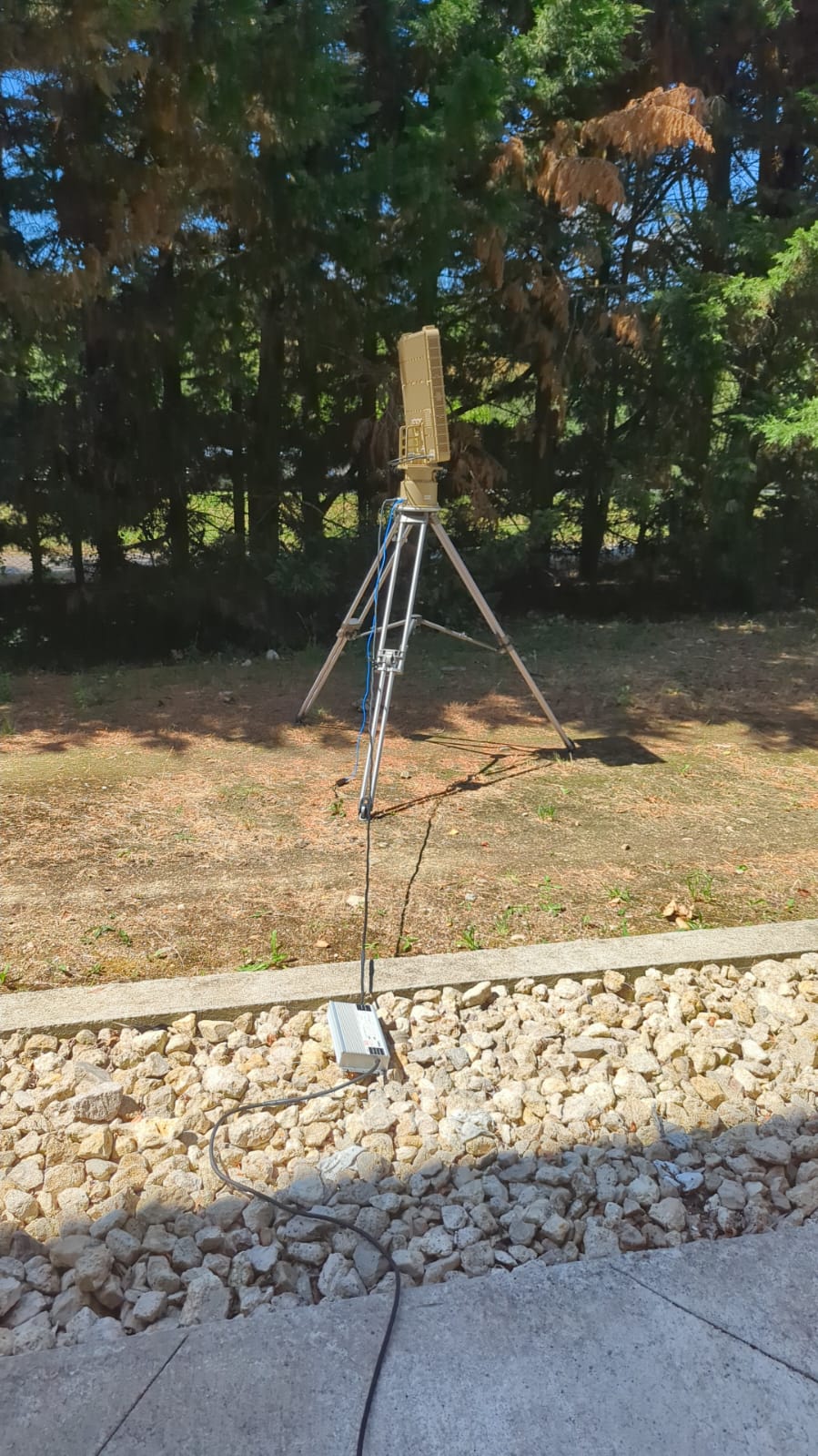
|
|
||||||
|
|
||||||
AERIS-10 is an open-source, low-cost 10.5 GHz phased array radar system featuring Pulse Linear Frequency Modulated (LFM) modulation. Available in two versions (3km and 20km range), it's designed for researchers, drone developers, and serious SDR enthusiasts who want to explore and experiment with phased array radar technology.
|
||||||
|
|
||||||
@@ -47,13 +46,13 @@ The AERIS-10 main sub-systems are:
|
|||||||
|
|
||||||
- **Main Board** containing:
|
- **Main Board** containing:
|
||||||
- **DAC** - Generates the RADAR Chirps
|
- **DAC** - Generates the RADAR Chirps
|
||||||
- **2x Microwave Mixers (LT5552)** - For up-conversion and IF-down-conversion
|
- **2x Microwave Mixers (LTC5552)** - For up-conversion and IF-down-conversion
|
||||||
- **4x 4-Channel Phase Shifters (ADAR1000)** - For RX and TX chain beamforming
|
- **4x 4-Channel Phase Shifters (ADAR1000)** - For RX and TX chain beamforming
|
||||||
- **16x Front End Chips (ADTR1107)** - Used for both Low Noise Amplifying (RX) and Power Amplifying (TX) stages
|
- **16x Front End Chips (ADTR1107)** - Used for both Low Noise Amplifying (RX) and Power Amplifying (TX) stages
|
||||||
- **XC7A50T FPGA** - Handles RADAR Signal Processing on the upstream FTG256 board:
|
- **XC7A50T FPGA** - Handles RADAR Signal Processing on the upstream FTG256 board:
|
||||||
- PLFM Chirps generation via the DAC
|
- PLFM Chirps generation via the DAC
|
||||||
- Raw ADC data read
|
- Raw ADC data read
|
||||||
- Digital Gain Control (host-configurable gain shift)
|
- Hybrid Automatic Gain Control (AGC) — cross-layer FPGA/STM32/GUI loop
|
||||||
- I/Q Baseband Down-Conversion
|
- I/Q Baseband Down-Conversion
|
||||||
- Decimation
|
- Decimation
|
||||||
- Filtering
|
- Filtering
|
||||||
@@ -68,13 +67,13 @@ The AERIS-10 main sub-systems are:
|
|||||||
- Clock Generator (AD9523-1)
|
- Clock Generator (AD9523-1)
|
||||||
- 2x Frequency Synthesizers (ADF4382)
|
- 2x Frequency Synthesizers (ADF4382)
|
||||||
- 4x 4-Channel Phase Shifters (ADAR1000) for RADAR pulse sequencing
|
- 4x 4-Channel Phase Shifters (ADAR1000) for RADAR pulse sequencing
|
||||||
- 2x ADS7830 ADCs (on Power Amplifier Boards) for Idq measurement
|
- 2x ADS7830 8-channel I²C ADCs (Main Board, U88 @ 0x48 / U89 @ 0x4A) for 16x Idq measurement, one per PA channel, each sensed through a 5 mΩ shunt on the PA board and an INA241A3 current-sense amplifier (x50) on the Main Board
|
||||||
- 2x DAC5578 (on Power Amplifier Boards) for Vg control
|
- 2x DAC5578 8-channel I²C DACs (Main Board, U7 @ 0x48 / U69 @ 0x49) for 16x Vg control, one per PA channel; closed-loop calibrated at boot to the target Idq
|
||||||
- GPS module for GUI map centering
|
- GPS module (UM982) for GUI map centering and per-detection position tagging
|
||||||
- GY-85 IMU for pitch/roll correction of target coordinates
|
- GY-85 IMU for pitch/roll correction of target coordinates
|
||||||
- BMP180 Barometer
|
- BMP180 Barometer
|
||||||
- Stepper Motor
|
- Stepper Motor
|
||||||
- 8x ADS7830 Temperature Sensors for cooling fan control
|
- 1x ADS7830 8-channel I²C ADC (Main Board, U10) reading 8 thermistors for thermal monitoring; a single GPIO (EN_DIS_COOLING) switches the cooling fans on when any channel exceeds the threshold
|
||||||
- RF switches
|
- RF switches
|
||||||
|
|
||||||
- **16x Power Amplifier Boards** - Used only for AERIS-10E version, featuring 10Watt QPA2962 GaN amplifier for extended range
|
- **16x Power Amplifier Boards** - Used only for AERIS-10E version, featuring 10Watt QPA2962 GaN amplifier for extended range
|
||||||
@@ -92,7 +91,7 @@ The AERIS-10 main sub-systems are:
|
|||||||
### Processing Pipeline
|
### Processing Pipeline
|
||||||
|
|
||||||
1. **Waveform Generation** - DAC creates LFM chirps
|
1. **Waveform Generation** - DAC creates LFM chirps
|
||||||
2. **Up/Down Conversion** - LT5552 mixers handle frequency translation
|
2. **Up/Down Conversion** - LTC5552 mixers handle frequency translation
|
||||||
3. **Beam Steering** - ADAR1000 phase shifters control 16 elements
|
3. **Beam Steering** - ADAR1000 phase shifters control 16 elements
|
||||||
4. **Signal Processing (FPGA)**:
|
4. **Signal Processing (FPGA)**:
|
||||||
- Raw ADC data capture
|
- Raw ADC data capture
|
||||||
@@ -111,7 +110,8 @@ The AERIS-10 main sub-systems are:
|
|||||||
- Map integration
|
- Map integration
|
||||||
- Radar control interface
|
- Radar control interface
|
||||||
|
|
||||||
|

|
||||||
|
<!-- V6 GIF removed — V6 is deprecated. V65 Tk and V7 PyQt6 are the active GUIs. -->
|
||||||
|
|
||||||
## 📊 Technical Specifications
|
## 📊 Technical Specifications
|
||||||
|
|
||||||
|
|||||||
@@ -32,6 +32,11 @@
|
|||||||
</section>
|
</section>
|
||||||
|
|
||||||
<section class="stats-grid">
|
<section class="stats-grid">
|
||||||
|
<article class="card stat notice">
|
||||||
|
<h2>Production Board USB</h2>
|
||||||
|
<p class="metric">FT2232H (USB 2.0)</p>
|
||||||
|
<p class="muted">50T production board uses FT2232H. FT601 USB 3.0 is available on 200T premium dev board only.</p>
|
||||||
|
</article>
|
||||||
<article class="card stat">
|
<article class="card stat">
|
||||||
<h2>Tracked Timing Baseline</h2>
|
<h2>Tracked Timing Baseline</h2>
|
||||||
<p class="metric">WNS +0.058 ns</p>
|
<p class="metric">WNS +0.058 ns</p>
|
||||||
|
|||||||
Reference in New Issue
Block a user